


Device fabrication
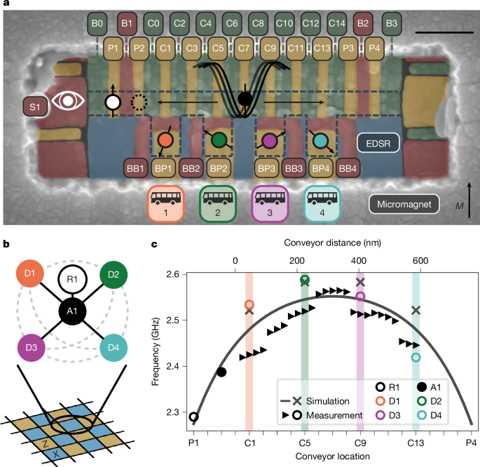
The device is fabricated on an isotopically purified 28Si/SiGe heterostructure containing a 7-nm-thick strained quantum well19, 30-nm SiGe buffer passivated with an amorphous silicon cap, and a 10-nm atomic layer deposition of insulating Al2O3. The heterostructure is nominally equal to that in previous studies where large average valley splitting in excess of 200 μeV (ref. 19) and high-fidelity shuttling5 have been observed. The four proceeding Ti:Pd layers have thicknesses of 3:17 nm, 3:27 nm, 3:27 nm and 3:27 nm respectively and are each followed by 5-nm atomic layer deposition of Al2O3. Finally, a 3:150 nm Ti:Co micromagnet is evaporated. The gate layer order is selected (refer to Fig. 1a) to maximize the tunnel coupling tunability for two-qubit interactions between the ancilla and data qubits as well as the interaction between the PSB pair, as gates in higher layers typically exhibit lower lever arms to the buried quantum well51.
Experimental set-up
The experiments were performed in an Oxford Instruments ProteoxMX dilution refrigerator where the mixing chamber temperature was held at 200 mK to mitigate heating effects52. A driven superconducting vector magnet was used to magnetize the on-chip micromagnet in a field of 1 T and is otherwise unpowered. The device was glued with GE varnish to a copper plate in direct thermal contact with the mixing chamber and was wirebonded to an in-house printed circuit board (PCB). We applied DC bias voltages supplied by battery-powered home-built voltage source modules (D5a) and generated baseband control and readout pulses with a Qblox Cluster equipped with eight 4-channel QCM arbitrary waveform generator (AWG) modules and a QRM module for RF reflectometry readout. DC channels were filtered with a combination of PI and RC filters with a nominal cut-off frequency of about 20 Hz. Alternating current (AC) channels were filtered by ferrite chokes, passed through UT85 stainless steel semi-rigid coaxial cables and attenuated by 20 dB at 4 K to balance thermalization and have a large dynamic range for baseband pulsing. The ±2.5 V output range of the AWG channels corresponded to a ±500 mV available range at the device. The DC and AC signals were combined through bias tees with a time constant of 100 ms. Two channels of a QCM module are used for IQ modulation of a Rohde & Schwarz SGS100A vector source. We set the local oscillator of the vector source to 2.27 GHz to ensure that all target qubit frequencies fall on the same sideband within the 400-MHz bandwidth of the QCM. The output power of the vector source was set to 6 dBm.
The RF tone for readout was generated by the QRM, attenuated by 40 dB at room temperature and 20 dB at 4 K, and the input and output signals passed through a MiniCircuits ZEDC-15-2B directional coupler at the mixing chamber stage. The input power was set to optimize the signal-to-noise ratio of charge sensing. The output signal was carried through a superconduting NbTi UT85 cable to a Cosmic Microwave Technologies CMT-BA1 cryogenic amplifier mounted at the 4 K stage, which provides approximately 30 dB of amplification. The signal was further amplified at room temperature with a home-built amplifier (standalone M2j), which provided an additional 45 dB of amplification before being filtered, digitized and demodulated by the QRM. The demodulated signal was digitally rotated to the in-phase component to make use of real-time feedback.
Initial device testing and tuning procedure
After cooling below 1 K, RF reflectometry was verified by finding the LC circuit resonances with a spectrum analyser. We then proceeded to verify DC transport through both SET structures as well as the conveyor channel. This is shown for the latter in Supplementary Fig. 4. Although the adjacent bus-stop gates cannot pinch off the channel entirely, their large effect on the conducted current is an indication that they operate normally, as shown in Supplementary Fig. 5. After verifying DC transport, we benefited from a complete thermal cycle to reset hysteresis before tuning up sensors with RF reflectometry.
The pinch-off voltages within the channel provide a first guideline for DC voltages that allow the device to be accessible by shuttling. We find that the channel gates in the same layer pinch off with reasonable uniformity around 1 V. To avoid unwanted static charge accumulation under the conveyor, we therefore set their preliminary DC voltages in the range of 700–800 mV. As the DC tests on the bus-stop gates do not provide such a quantitative guideline, we rely on electrostatic simulations to estimate the bus-stop gate voltages needed to create a balanced double-dot potential with the corresponding conveyor gate. We extract roughly a factor 1.5 and 1 for the bus-stop plunger and barrier, respectively, compared with the conveyor gate voltages. We therefore set the bus-stop plungers to 1,200 mV and the bus-stop barriers to 750 mV as a reasonable starting point to tune the array.
After verifying DC functionality, the device tune-up proceeds in the following sequence: (1) ancilla readout and control, (2) coarse conveyor-mode shuttling, (3) single-spin remote tuning and virtual gate matrix calibration, (4) spin reloading, (5) two-spin remote tuning and exchange detection, (6) optimization of coherent conveyor-mode shuttling, (7) CROT tuning and implementation of the QND measurement framework, and (8) single- and two-qubit gate calibration.
Ancilla readout
Charge sensing was achieved via an RF SET measurement. The 2D electron gas (2DEG) leads of each SET were accumulated according to the split-gate method, where the RF signal was capacitively coupled to the 2DEG via an accumulation gate to minimize series resistance and remove leakage pathways53. An LC tank circuit was formed with a NbTiN meandering superconducting nanowire with a nominal kinetic inductance on the order of a few microhenry, the series capacitance between the accumulation gate and the 2DEG, and the parasitic capacitance between the bond wires and the PCB ground plane, giving rise to a resonance frequency of 114.3 MHz.
Spin-to-charge conversion was achieved via parity-mode PSB. The Zeeman energy difference of about 100 MHz between the readout ancilla R1 and ancilla A1 lifts the blockade of the \(|T_\rangle \) spin triplet, resulting in an effective Z ⊗ Z observable for the qubit pair54. The (4, 0)–(3, 1) interdot charge transition was used such that R1 occupies the dot where the lowest valley–orbit shell is filled, increasing the energy required to lift the blockade. A charge stability diagram of this region can be seen in Supplementary Fig. 7b.
PSB was first tuned in isolation mode, where the tunnel barrier to the reservoir (S1) was completely closed, as this makes the visual characteristic easier to recognize during manual tuning with video-mode charge-state measurements while sweeping the respective plunger gates of the PSB pair. After initial identification of the qubit resonances, PSB was retuned with a finite reservoir coupling to allow for efficient qubit reloading.
The tunnel coupling between the quantum dots of the readout pair was pulsed to be on the order of several gigahertz such that the singlet state \(|S(4,0)\rangle \) evolves adiabatically to the \(|\uparrow \downarrow \rangle \) spin state of the (3, 1) configuration with a 50-ns linear voltage ramp. This allows for the initialization of an unblockaded \(|\uparrow \downarrow \rangle \) state via post-selection. Real-time feedback serves to enhance the fraction of post-selected measurement shots by flipping the state of A1 if blockade is detected during initialization. Although we conceptually identify the ancilla qubit as the single-spin A1 that is shuttled through the device, it is technically correct to attribute the qubit to the parity of the \(|R_1\rangle \otimes |A_1\rangle \) spin state. The initialization and readout protocols of Fig. 3 only require PSB to be parity-preserving to function correctly.
After achieving reasonable readout visibility with manual tuning, the visibility of Rabi oscillations was used as a cost function for a CMA-ES optimizer to maximize the quality of initialization and readout55. The optimizer takes as parameters the voltage pulse amplitudes on all gates immediately surrounding the double-quantum-dot system hosting the readout pair, as well as the durations of piecewise-linear voltage ramps defining the readout sequence. We routinely achieve ancilla qubit visibilities of about 97% with such an optimization, corresponding to initialization and readout error rates of about 1%, while using an integration time of 10 μs. The integration time is selected such that spin readout is stable over periods of at least 1 day without requiring more frequent recalibration. We note that similar performance can be achieved by shortening the integration time to as low as 5 μs at the expense of requiring more interleaved threshold calibrations. In the future, the optimal integration time must balance the quality of readout with the dephasing incurred by other spins during coherent mid-circuit measurements.
Conveyor-mode shuttling
To generate the travelling-wave potential for the shuttling bus, we make use of a four-phase conveyor-mode pulse template as in refs. 3,5,7,41. The goal is to generate a smooth moving-dot potential that minimizes the decoherence of a shuttled spin42,56,57,58,59. During conveyor operation, every participating virtual gate vG ∈ vC0, … vC12, vU1, vϵ1, …, vU4, vϵ4 is assigned a voltage vG such that:
$$vG(t)=vG^\mathrmoffset+vG^\mathrmamp\sin (2\rm\pi f_\mathrmconvt-\phi _G),$$
(1)
where ϕG = mπ/2 for integer m ∈ 0,1,2,3 such that every fourth virtual gate is in-phase. vU1−4 and vϵ1−4 are used in place of vC1, vC5, vC9 and vC13 to avoid unwanted charge transitions at the bus stops during shuttling. All gate voltages oscillate with the conveyor frequency fconv, and the constant offsets vGoffset and amplitudes vGamp are unique to each individually controlled gate. The set of parameters fconv, vGoffset, vGamp constitutes a conveyor definition. The pulses are applied in addition to the constant DC bias voltages vGDC.
All shuttling experiments begin with the ancilla A1 located below P2. A linear voltage ramp to vG(0) pulls the charge below C0, and the travelling-wave potential minimum progresses by four gate lengths for every conveyor cycle of duration tconv = 1/fconv. The ancilla is therefore localized adjacent to bus stops 1–4 at t/tconv = 0.25, 1.25, 2.25, 3.25, respectively. When the conveyor voltages are held constant at a fixed time, additional gate voltage pulses (for example, for activating an exchange interaction) are applied in linear combination with the paused conveyor. The direction of the travelling-wave potential is reversed by flipping the sign of fconv and adding a time-dependent offset to ensure that there is no sudden discontinuity in the conveyor. The charge returns from below C0 to below P2 by linearly ramping all conveyor voltages to zero.
Two conveyor definitions are used during the operation of the array. The first is a coarse-tuned conveyor that is used to shuttle uninitialized spins past unpopulated bus stops during loading and unloading. This is achieved by manually tuning vGamp and, if necessary, the DC gate voltages, to ensure good charge shuttling fidelity. Coherent spin-shuttling fidelity is unimportant for this conveyor definition. The coarse conveyor is tuned by using adiabatic inversion to infer the movement of the spin in the inhomogeneous magnetic field.
The second conveyor definition is used when the bus stops are loaded with single electrons, and therefore the electrostatic landscape of the bus is different than during loading (which is ordered from bus stop 4 to bus stop 1 to avoid this issue). Here, coherent spin transfer is relevant, and we make use of CMA-ES optimization to fine-tune vGoffset, vGamp. As a cost function, we use an echo-type experiment where the spin is shuttled ten times back and forth in total from P2 to C1355. The spin visibility serves as a proxy for the dephasing experienced during shuttling, making it an easy-to-evaluate cost function for optimization.
The Larmor frequencies along the optimized conveyor, as shown in Fig. 1c, are extracted by preparing the shuttled spin in superposition and observing the precession frequency after transporting the spin to various points along the array.
Single-spin remote tuning
After confirming the operation of the shuttling bus, the loading protocol of the bus stops can be tuned. For this, we leverage the availability of EDSR throughout the bus to perform Ramsey experiments with respect to various rotating frames, but we note that the strategy we use is compatible with not having single-spin control throughout the array. The minimum requirement is the ability to prepare a spin in a superposition state and shuttle it coherently.
During initial tuning, no gate virtualization has taken place beyond the readout zone, and the ability to load the bus stops is probed by applying a physical detuning pulse ϵi = Cj − BPi where Cj is the voltage of the conveyor gate adjacent to bus stop i (j = 1, 5, 9, 13 for bus stops 1–4 respectively). Extended Data Fig. 1a–d shows the first convincing experimental signatures of bus-stop loading before any virtualization takes place. To verify that the bus stop is the most likely destination for the tunnelled electron, we repeat the loading experiments while pulsing negatively on the surrounding conveyor gates. This provides evidence that tunnelling is not taking place within the shuttling bus.
The Larmor frequency difference between the spin when localized in the bus and in the bus stop encodes information about its position in the phase of the spin state. For each bus stop, we select a free evolution time on the order of tens of nanoseconds to optimize contrast between the two cases, and we use this signal to virtualize control of the effective double-dot system as well as the surrounding conveyor gates. First, we focus on the gate voltage subspace consisting of the physical conveyor gate voltage Cj and physical bus-stop plunger gate voltage BPi. In the case of bus stop 1, these gates are already virtualized with respect to the readout zone, but not to each other, and the following procedure is the same regardless of any pre-existing virtualization.
We define unvirtualized detuning and average potential parameters ϵi, Ui that relate to voltages Cj, BPi as \((\epsilon _i,U_i)^\rmT=V(Cj,\rmB\rmPi)^\rmT\) where:
$$V=\left(\beginarrayrc1 & -1\\ 0.5 & 0.5\endarray\right).$$
(2)
We want to identify corresponding virtual gates vCj and vBPi, where (vCj, vBPi)T = Mi(vCj, BPi)T, such that the virtual detuning and average potential, defined as (vϵi, Ui)T = V(vCj, vBPi)T, relate to the double-dot chemical potentials as sketched in Fig. 2a. Explicitly, this means vϵi ∝ μCj − μBPi and vUi ∝ (μCj + μBPi)/2 where μCj and μBPi are the chemical potentials of the dots formed below gates Cj and BPi, respectively. An interdot charge transition to bus stop i should therefore only be modulated by vϵi.
The interdot charge transitions measured when sweeping the physical detuning and average potential parameters (Supplementary Fig. 6a) show a finite (positive) slope \(\rmd\epsilon _i/\rmdU_i=\tan \theta _i\) from which it follows that \((v\epsilon _i,vU_i)^\rmT=R(\theta _i)(\epsilon _i,U_i)^\rmT\) where R(θi) is an anticlockwise rotation about the origin \((\epsilon _i=v\epsilon _i=0,U_i=vU_i=0)\) by an angle θi. We therefore have Mi = V−1R(θi)V. Applying the elements of Mi to the total virtual gate matrix permits direct control over the virtual detuning and average potential.
To virtualize any other gate G with respect to each bus-stop plunger BPi, the same experiment definition is used where the slope dBPi/dG of the interdot transition informs both the degree of influence of the gate voltage G on the chemical potential below gate BPi and therefore the virtual gate definition vG required to offset the effect (Supplementary Fig. 6b). The slope \(\mathrmdBPi/dCj=(2-\tan \theta _i)/(2+\tan \theta _i)\). This provides all slopes plotted in the crosstalk heatmap of Fig. 2g.
Extended Data Fig. 1e–h shows the loading experiments repeated after gate virtualization has taken place. In certain cases, the tunnel coupling between the bus and bus-stop dots is pulsed during tunnelling to smoothen the transition compared with the preliminary loading. The two-electron charge stability diagrams reconstructed from the shuttled spin polarization in Extended Data Fig. 1i–l also show charge transitions that are effectively orthogonal to the virtualized detuning axis, confirming the validity of this approach.
We estimate that this remote-tuning strategy would be sufficient to tune on the order of 100 qubits at bus-stop-like locations in a sparse quantum-dot array. Taking a trilinear quantum-dot array as an example49,50, with the central row operated as a shuttling channel, we could envision placing a single charge sensor and reservoir at one end and shuttling a distance on the order of 10 μm. As demonstrated in ref. 5, coherent spin shuttling with high fidelity over such a distance should be possible, although we emphasize that high fidelity is not necessary for our remote-tuning protocol to function. On the basis of our device geometry, we estimate that a total of 110 bus stops would fit adjacent to such a shuttling channel. With a shuttling speed of 50 m s−1 and a spin reload time on the order of 1 μs, loading every bus stop would require about 120 μs. Even with AC loading, this timescale is still well within the 100-ms bias-tee time of our sample board.
In this extreme example, qubit measurement for the purposes of quantum information processing would be impractically slow. However, it illustrates that shuttling can be used to massively multiplex tuning and qubit readout well beyond what is currently possible with dense spin arrays.
Spin reloading
Supplementary Fig. 7a illustrates the procedure used for reloading a new spin into the array after the original ancilla has been shuttled to occupy a bus stop. The sensor S1 doubles as an electron reservoir from which qubits can be loaded on-demand. It has a small but finite tunnel coupling to the dot below P1 where the readout ancilla R1 remains and a weaker coupling to the dot below P2 where the ancilla A1 is initialized as can be seen in the measured charge stability diagram of Supplementary Fig. 7b.
After shuttling the ancilla, the voltage configuration in the readout zone remains at the operation point O in the quasi-equilibrium (3, 0) charge state. As the direct tunnel rate to (3, 1) is very slow, this charge configuration persists for at least 20 ms and is limited by the bias-tee charging time of the sample PCB. No unwanted electrons tunnel into the empty dot during the experiments. To reload on-demand, the virtual detuning of the readout pair vϵR is pulsed to the reload point R. The rate at which a new charge enters is evident from Supplementary Fig. 7c. Pulsing beyond the PSB region of the interdot transition allows for a relatively fast loading to the (4, 0) state in less than 10 μs, and ramping the detuning back to O returns the system to the equilibrium (3, 1) charge state and restores the ancilla spin. No additional barrier pulse (that is, on gate B0) is used to modulate the tunnel rate, and including one could increase the loading speed further. This reloading procedure repeats until all bus stops are occupied and the final ancilla spin is reloaded, after which the initialization protocol may begin.
The bus-stop spins are unloaded in one of two ways. First, they may be shuttled back to the readout zone in a sequence inverse to the loading protocol. In this case, the 5-electron charge state at the readout zone quickly equilibrates to the (3, 1) charge state in about 1 μs, and no detuning pulse is necessary. Alternatively, we can simply ramp all pulsed voltages back to their DC condition without any travelling-wave potential used. Bias-tee compensation pulses are applied over a period of several tens of microseconds before the next experimental shot begins, and the free spins vacate the bus stops within this timescale, presumably to one of the 2DEG reservoirs on either side of sparse array. We observe no adverse consequences when unloading spins in this manner, and this approach is used for most experiments presented in this work.
The necessity for unloading and subsequent loading is set by the finite bias-tee time and amplitude range of the AWG modules. In future work, loading bus stops or other remote quantum dots with DC voltages would eliminate the need for spin reloading altogether.
QND measurement
All qubits in the effective five-qubit processor can be measured in the computational basis as illustrated in Fig. 3d by a sequence of parity-mode PSB measurements m0, m1, m2, …. We use the convention that each projective measurement ideally yields mk = +1 when an odd-parity spin state \(|R_1\rangle \otimes |A_1\rangle \) is present and mk = −1 when an even-parity spin state is present.
The ancilla is always measured first. By assuming that R1 remains in the prepared eigenstate \(|1\rangle \) throughout all experiments, m0 = a1 gives the computational-basis measurement outcome of qubit A1. To perform a QND measurement on a data qubit Di, A1 is shuttled adjacent to the relevant bus stop and a calibrated CROT will flip the state of A1 conditional on the data qubit being in the \(|1\rangle \) state. The next measurement mk indicates whether an ancilla spin-flip took place by considering the previous measurement mk−1. The kth computational-basis readout di,k of Di is therefore given by the product mk−1mk.
Unlike for the ancilla measurement, repeated QND measurements can take place on the data qubits to improve the readout fidelity as indicated in Fig. 3a. To characterize the quality of the repeated QND readout, we perform Rabi oscillation measurements with 20 sequential QND readouts on the 4 data qubits individually. Extended Data Fig. 2a gives an exemplary circuit for D2. The QND single-shot outcomes di = di,1, di,2, …, di,20 are used to infer the data qubit Di \(|1\rangle \) state probability P1(tb) through a majority-vote scheme. The resulting oscillation is fit to \(P_1(t_\rmb)=B-A\cos (2\rm\pi f_\rmRt_\rmb)\exp (-t_\rmb/T_2^\rmR)\), where tb is the microwave burst time, fR is the Rabi frequency, and \(T_2^\rmR\) is the Rabi oscillation decay time. Extended Data Fig. 2b shows the visibility, given by 2A, of the Rabi oscillations as a function of the number of QND readout cycles used in the majority vote. We use up to five QND repetitions in our experiments, as this yields the highest visibility for all data qubits.
We also characterize the QND fidelity of our readout, which quantifies the ability of the QND measurement to preserve the data qubit \(|0\rangle \) and \(|1\rangle \) states. We again utilize the 20 repetitive QND readouts but calculate the Rabi oscillation from each individual outcome di,k. This results in Rabi oscillations with decaying amplitudes and offsets as the data qubit state is disturbed by finite CROT fidelity and spin relaxation. The individual Rabi oscillations P1,k(tb) are fitted to obtain the amplitude Ak and offset Bk for the kth QND measurement repetition. The decay of these parameters is then fitted using the model60:
$$A_k=A_\gamma ^k,$$
(3)
$$B_k=\left(B_-\frac1-\gamma _1-\gamma \right)\gamma ^k+\frac1-\gamma _1-\gamma ,$$
(4)
where \(\gamma _=\exp (-t_\mathrmQND/T_1^(0))\), \(\gamma _1=\exp (-t_\mathrmQND/T_1^(1))\) and γ = γ0 + γ1 − 1. tQND is the time required for a cycle of QND measurement, which in our case is about 12 μs for all four data qubits, \(T_1^(0)\) is the spin-flip time of the data qubit \(|0\rangle \) state, and \(T_1^(1)\) is the spin-flip time of the data qubit \(|1\rangle \) state. We observed a decay in Ak for all data qubits. However, only data qubit D4 shows a decay in Bk; the remaining data qubits show no visible decay over the 20 QND repetitions. We conclude that the QND readouts of D1, D2 and D3 are mainly limited by unintentional data qubit spin flips owing to the CROT infidelity, whereas the QND readout of D4 is affected by both the CROT infidelity and intrinsic spin relaxation. We are unsure of the reason for this unique spin relaxation effect. One possible explanation could be that the valley splitting of the dot containing D4 is nearly degenerate with the Zeeman splitting, as spin relaxation would be enhanced. Although T1 times were not measured in this device, we would expect them to be on the order of hundreds of milliseconds based on measurements in similar devices. This potential issue may be bypassed by changing the magnetic field to lift the degeneracy.
The fitted parameters Ak and Bk are related to the QND fidelities by the following relation60:
$$P_1,k(t_\rmb)=(1-F_0,k^\mathrmQND)(1-P_1,0(t_\rmb))+F_1,k^\mathrmQNDP_1,0(t_\rmb),$$
(5)
which translates to:
$$F_0,k^\mathrmQND=1-B_k+\fracB_A_A_k,$$
(6)
$$F_1,k^\mathrmQND=B_k+\frac1-B_A_A_k.$$
(7)
Figure 2c shows the extracted QND fidelities \(F_0,k^\rmQND\) and \(F_1,k^\rmQND\), along with the average fidelity \(F_\rmavg,k^\rmQND=(F_0,k^\rmQND+F_1,k^\rmQND)/2\). For one QND repetition, the \(F_\rmavg,1^\rmQND\) for D1–D4 are 96.7(1.8)%, 99.2(1.7)%, 99.1(1.3)% and 96.1(1.4)%, respectively.
Universal spin control
All primitive qubit operations can be derived from the Heisenberg Hamiltonian describing the sparse spin array. It can be expressed in terms of the Loss–DiVincenzo qubit operators as:
$$H=\sum _ijhJ_ij\left(\frac\boldsymbol\sigma _i\cdot \boldsymbol\sigma _j4-\frac14\right)-\sum _i\frac12g\mu _\rmB\bfB_i\cdot \boldsymbol\sigma _i,$$
(8)
where \(\boldsymbol\sigma _i=(X,Y,Z)^\rmT\) is the vector of Pauli matrices acting on qubit i, Bi is the magnetic-field vector at the location of qubit i, h is the Planck constant, g ≈ 2 is the electron spin g-factor in silicon, and μB is the Bohr magneton. Jij gives the magnitude of the exchange interaction between spins. It is controllable via baseband pulses on the electrostatic gates and is effectively zero for non-adjacent spins.
When J = 0, single-qubit control is achieved via EDSR where an oscillating electric field \(E_\mathrmac(t)\cos (2\rm\pi f_\mathrmMWt+\phi )\) with time-varying amplitude Eac(t), frequency fMW and phase ϕ couples to the spin via a transverse gradient bt originating from the micromagnet stray field. The single spin therefore experiences an effective magnetic field \(\bfB(t)=(hf_\rmR\cos (2\rm\pi f_\mathrmMWt+\phi ),0,hf_\rmL)^\rmT/g\mu _\rmB\) where fL is the Larmor frequency set by the total magnetic field at the qubit location and \(f_\rmR(t)=g\mu _\rmBb_teE_\mathrmac(t)a_^2/2hE_\mathrmorb\) is the on-resonance Rabi frequency, e is the electron charge, a0 is the Fock–Darwin length scale of the quantum dot and Eorb is the orbital energy scale of the quantum dot.
In the rotating frame, the single-qubit Hamiltonian after application of the rotating wave approximation is:
$$H_\mathrmEDSR=\frach(f_\mathrmMW-f_\rmL)2Z+\frachf_\rmR(t)2(\cos \phi X-\sin \phi Y),$$
(9)
When driven on-resonance such that fMW = fL, the single-qubit unitary evolution is given by
$$U_1\rmQ=\exp (-\rmi2\rm\pi f_\rmR(t)t(\cos \phi ,-\sin \phi ,0)^\rmT\cdot \boldsymbol\sigma /2),$$
(10)
which is a rotation \(R_\widehatn(\theta )\) about an axis \(\widehatn=(\cos \phi ,-\sin \phi ,0)^\rmT\) by an angle θ = 2πfR(t)t. All single-qubit gates are derived from a single definition for an \(X_90=\exp (-\mathrmi\pi X/4)\) operation, which consists of a microwave burst of duration t90. Rotations around other axes are implemented by changing the phase ϕ of the microwave burst, and arbitrary rotations Rz(θ) about the z axis of the Bloch sphere are similarly implemented by a phase update of the subsequent microwave bursts. X180 rotations are implemented with two concatenated X90 pulse definitions. The use of a unique single-gate primitive streamlines the calibration of crosstalk in the multi-qubit Hilbert space.
As all microwaves are delivered via a single antenna, we rely on spectral separation to address individual spins. To limit errors owing to off-resonant coherent driving, we use a Hamming window for the microwave pulse amplitude Eac(t) to limit the bandwidth of each microwave pulse to approximately 1/t90. For pulse durations of about 250 ns, the pulses therefore have a resolution of about 10 MHz. The remaining phase pickup owing to the AC Stark shift and heating effects is calibrated experimentally and accounted for in the form of virtual phase updates.
A CROT operation is used for initialization and readout by applying a resonant pulse while the exchange Jij between the shuttled ancilla and a data qubit is finite. In the limit where the exchange is much smaller than the Larmor frequency difference between spins (\(J_ij\ll | f_\rmL,i-f_\rmL,j| \)), it is appropriate to approximate the resonance frequency of qubit i as conditional on the state of qubit j with a separation of Jij. Qubit i can therefore be conditionally rotated depending on the state of qubit j via EDSR. The exchange Jij(t) is ramped on and off adiabatically with a Tukey pulse shape, and a microwave burst with a rectangular window is applied for a duration t180 required for a complete flip of qubit i. The synchronization condition \(1/2t_180=J_ij/\sqrt4n^2-1\) with integer n is used to drive a 2π rotation in the subspace of the undesired transition61. The operation therefore performs the mapping \(\01\rangle ,\) which is suitable for a projective QND measurement of the control qubit in the computational basis. Although the CROT may form a universal entangling gate, we do not use the CROT as a coherent two-qubit operation and therefore do not track the single-qubit phases picked up during the operation. We also neglect the conditional phases in the CROT as they are unimportant for initialization and readout.
Coherent two-qubit operations are implemented by modulating the exchange Jij adiabatically without any additional microwave burst. This ideally results in a unitary evolution \(U_2\rmQ=\mathrmdiag(1,\rme^-\rmi\phi _01,\rme^-\rmi\phi _10,\rme^-\rmi\phi _11)\). U2Q can be transformed into a controlled-phase gate via commuting virtual single-qubit z rotations such that \(R_z(\phi _10)\otimes R_z(\phi _01)U_\mathrm2Q\,=\) \(\mathrmdiag(1,1,1,\rme^\rmi(\phi _01+\phi _10-\phi _11))\). A controlled S gate between qubits i and j is achieved when Jij(t) is modulated such that ϕ01 + ϕ10 − ϕ11 = π/2. The duration for the gate is bounded by \(t_\mathrmCS > 1/4J_ij,\max \), where Jij,max is the maximum exchange strength during the operation, and is necessarily longer to maintain adiabaticity.
The CS gate is used as the two-qubit entangling primitive as illustrated in Fig. 4a where the single-qubit z rotations are obviated by the refocusing pulses. The multi-qubit DCZ operation can be expressed in terms of controlled-phase gates \(\mathrmCZ_00^i\) acting on the ancilla qubit and data qubit i, where \(\rmCZ_xy|m,n\rangle =(-1)^\delta (x,m)\delta (y,n)|m,n\rangle \). The circuit of Fig. 4a implements the unitary \(X_180^\otimes (w+1)\Pi _i=1^w\mathrmCZ_00^i\) acting on the ancilla qubit and w data qubits. With a universal single-qubit gate set, this operation is sufficient to apply any Pauli operation on the data qubits, conditional on the state of the ancilla qubit.
Gate calibration protocols
Periodic calibration of the five-qubit processor is necessary to compensate for slow drifts in the solid-state environment to maintain the gate fidelities required for the results presented in this work. We use a semi-automated calibration procedure that efficiently updates the control parameters for resonant gates (Supplementary Fig. 8), crosstalk compensation (Supplementary Fig. 9) and adiabatic two-qubit gates (Supplementary Fig. 10). The following protocols may be carried out once all bus stops can be populated, the ancilla can be shuttled with reasonable fidelity (specifically, the visibility of QND measurement of the data qubits will be bounded by how well spin polarization is preserved during shuttling), and all four exchange interactions are tunable over a workable range (for example, 100 kHz < J < 10 MHz).
Single-qubit gate and CROT calibration
Each resonant gate calibration begins with a coarse calibration followed by a finer one. We coarsely calibrate the Larmor frequency of the ancilla qubit A1 using microwave spectroscopy. The dip in the measured odd-state return probability is isolated and the resonance frequency is estimated via a quadratic fit. We then drive A1 with a microwave burst shaped by Hamming window of varying duration and we fit the Rabi oscillations to extract the current Rabi frequency \(f_\rmR^\rmfit\). As we aim for \(f_\rmR^\rmtarg=1\,\rmMHz\), or t90 = 250 ns, we rescale the driving amplitude by \(f_\rmR^\rmtarg/f_\rmR^\rmfit\).
A finer calibration is then performed using a Ramsey experiment, with the rotating frame virtually detuned by 1 MHz from the coarsely calibrated Larmor frequency. Fitting the resulting Ramsey oscillations yields a frequency correction. Finally, we fine-tune the 250-ns microwave burst amplitudes. The procedure applies multiple 2π qubit rotations (typically 4), each decomposed into 4 repeated X90 gates, to amplify any systematic over-rotation. The sequence is terminated with either an X90 or a X−90 gate to prepare the qubit in a superposition state. By sweeping the pulse amplitude, we select the value that yields a 50% odd-parity measurement probability for both final states (corresponding to ⟨Z⟩ = 0). The last two calibration steps are often iterated until they converge.
The CROT is calibrated using a four-step procedure, beginning with a coarse frequency estimation obtained by fitting a double-Gaussian function to an exchange spectroscopy trace acquired with the relevant data qubit in a mixed state and the exchange activated. This is possible before resonant control of the data qubits has been calibrated. For all CROTs, the higher-frequency branch is selected to drive the ancilla conditional on the data qubits occupying the \(|\uparrow \rangle \equiv |1\rangle \) state. The Rabi frequency of the CROTs is used to calibrate the driving amplitude required to meet the synchronization condition.
The coarse CROT calibrations are sufficient to initialize the data qubits using QND measurement and post-selection of the desired CROT outcome, and resonant control of D1–D4 may then be calibrated analogously to A1. A finer CROT calibration is then performed by initializing the data qubits to the \(|1\rangle \) state. The same calibrations are repeated, yielding more accurate estimates of both the conditional resonance frequency and the required drive amplitude owing to the improved trace visibility.
A finer calibration of the CROTs, along with resonant control of the data qubits, allows for higher visibility of the data qubits by using the full QND measurement framework presented in Fig. 3. Consequently, resonant control of the data qubits can be calibrated more precisely, and the process can be iterated until satisfactory convergence of the parameters has been achieved.
Single-qubit phase correction
As all resonant control signals are applied to the same screening gate, operating the device as a five-qubit processor requires mitigating crosstalk effects when driving different qubits that may arise owing to a combination of the AC Stark effect, device heating and induced shifts in the stray magnetic-field gradient. As the addressability gradient and pulse-shaping limit off-resonant rotations given by equation (10), this crosstalk predominantly manifests as phase pickup, which can be compensated for by virtual Rz(ϕ) gates.
To characterize these phases and determine the corresponding per-gate phase corrections, we perform a series of Hahn-echo-like experiments as shown in Supplementary Fig. 9a in which the target qubit remains idle while repeated sequences of X90 and X−90 gates are applied to each of the other qubits. We limit the number of applied gates to a maximum of N = 4 to remain in the linear regime, allowing us to extract the per-gate accumulated phase via a linear fit.
These induced phases can be compared with the predicted AC Stark shifts, showing partial qualitative agreement. However, the presence of self-induced phase accumulation (non-zero diagonal elements) as well as magnitude and sign discrepancies with the experimental data indicate that other effects, such as heating, have a significant role.
Adiabatic CS calibration
We calibrate coherent two-qubit interactions between the ancilla qubit and data qubits using an approach similar to ref. 21. The dynamic range of the exchange interaction is probed to find a suitable empirical relation Ji(vBBi) for all four bus stops. The charge-symmetry point is also identified via a fingerprint scan as an approximately linear function of the barrier voltage such that vϵi ∝ vBBi. This allows for pulse-shaping of the exchange strength Ji(t) to maximize the adiabaticity of the interaction while remaining robust to charge noise62,63.
Each effective CS operation is actuated by a series of baseband pulse segments as exemplified in Supplementary Fig. 10a. The first segment is a fast detuning ramp to the symmetry point. The second segment is a linear ramp to a subthreshold exchange magnitude (for example, J < 1 MHz). The central segment is a Hamming-shaped exchange modulation characterized by a pulse duration and magnitude vBBiON, which are selected to balance speed and adiabaticity. The remaining two segments are time-reversed copies of the first two to uncouple the qubits.
The pulse sequence in Supplementary Fig. 10b is used to fine-tune the amplitude vBBiON in a DCZ sequence such that the total conditional phase picked up by A1 can be identified for both computational-basis state preparations of the relevant data qubit Di. This is exemplified for the two-qubit interaction at bus stop 2 in Supplementary Fig. 10c,d. A total conditional phase difference of π is selected to ensure each individual CS operation accrues π/2 radians of conditional phase.
Single-qubit characterization
The dephasing times measured using CPMG decoupling can be used to gain insight into the noise spectrum influencing each qubit (Fig. 3e). We assume a monotonic noise spectrum S(ω) = A/ωα acting on each qubit such that \(T_2=T_2^N_\rm\pi ^\alpha /(1+\alpha )\) and \(T_2^=(2/A)^1/(\alpha +1)\rm\pi ^\alpha /(1+\alpha )\) and observe a good fit in all cases64. \(T_2^* \) measurements use a total integration time of about 25 minutes.
Single-qubit gate fidelities are evaluated using randomized benchmarking. We use the primitive gate set I, X90, Y90 of only positive rotations such that a Clifford gate is composed of 3.125 primitive gates on average65. A X90 gate duration of 250 ns is used for each primitive gate. The single-qubit Clifford gate fidelities are 98.98(3)%, 99.930(5)%, 99.90(1)%, 99.87(1)% and 99.924(6)% for A1, D1, D2, D3 and D4, respectively. Individual single-qubit gate fidelities in the single-qubit subspace are all well above 99.9% for the data qubits, and slightly lower for the ancilla qubit (Fig. 3g). We speculate that the lower ancilla fidelity may be due to its relative proximity to the reservoir, which is tunnel-coupled to R1 for the purposes of spin reloading. In the experiment, pairs of single-qubit operations were performed simultaneously when applicable. When all four bus stops were used, D1/D2 and D3/D4 were parallelized. When three bus stops were used, the ancilla would be driven in parallel with one of the bus stops.
To benchmark the shuttling performance, we use interleaved randomized benchmarking. The resonant control of qubit A1 when localized below P2 is used as the reference set. The interleaved operation consists of shuttling from below P2 to a location in the shuttling bus adjacent to a bus stop, idling for 50 ns, and shuttling back. A calibrated phase correction is added to make the targeted interleaved operation an identity gate. The measured fidelities do not change substantially with a small increase in the idling time; therefore, we believe that most of the infidelity originates during shuttling itself. A significant fraction of the shuttling error originates during loading and unloading the conveyor, when A1 moves from below gate P2 to below gate C0, as seen from the 97.9% round-trip shuttling fidelity to bus stop 1. This transition is induced with a linear voltage ramp of 40 ns duration and may be possible to optimize further. Only a 0.2% decrease in fidelity is observed when shuttling the remaining round-trip distance to bus stop 4. One round-trip of the ancilla from below P2 to bus stop 4, in the absence of any 2-qubit interactions, takes place in 730 ns. Considering that the \(T_2^\rmH\) of A1 is 47.6 μs with a decay exponent of 1.7 when localized below P2, we estimate that dephasing alone could contribute about 0.1% to the infidelity. Increasing the speed of the travelling-wave potential would be the most effective way to increase this limit (in ref. 5, conveyor speeds were up to 25 times faster).
To implement the refocusing pulse during the DCZ operation, we shuttle the ancilla back to below P2 as opposed to keeping the qubit adjacent to bus stop 4. This redundant shuttling adds 730 ns of shuttling and incurs an additional error of about 2.7%, much of which is picked up between P2 and C0. We include the redundant operation for three reasons. First, the Zeeman energy difference between the ancilla localized adjacent to bus stop 4 and data qubit D4 is relatively small, and therefore vulnerable to coherent errors if not calibrated at the synchronization condition. Second, we find that single-qubit EDSR driving within the conveyor potential does not always exhibit high fidelity, so optimizing high-fidelity control would require additional baseband pulses. Third, activating the conveyor shifts all qubit frequencies. For experimental ease of avoiding added calibration overhead, we opt to perform all single-qubit operations at the same voltage setpoint when the conveyor is deactivated.
We did not observe any clear evidence of valley excitations limiting the quality of the multi-qubit demonstration. For example, such excitations could result in observing two closely spaced resonance frequencies as spins occupying different valley–orbit states will have slightly different g-factors66,67. This effect was observed during the initial tuning of the exchange coupling of bus stop 1, but subsequent changes to the loading pulse sequence removed the effect.
It is understood that fluctuations in the valley splitting across a silicon shuttling channel can limit the quality of spin shuttling42,57,68. It is possible that we would be able to resolve such effects by further optimizing the shuttling channel and rigorously characterizing the valley splitting across the array.
Two-qubit characterization
We use character randomized benchmarking (CRB) to evaluate the performance of the two-qubit interaction between the shuttled ancilla and the four data qubits69. CRB allows us to use simultaneous single-qubit Clifford gates as the reference gate set as opposed to general two-qubit Clifford operations, which require many native CZ gates to compile.
As seen in Fig. 4a, the entangling interaction used to implement parity checks is a composite operation consisting of coherent shuttling, two-qubit interactions and single-qubit gates for refocusing phase pickup. Furthermore, we take advantage of the fact that the native controlled-phase interactions commute. We therefore benchmark each individual DCZ interaction to estimate the isolated error contribution from each component of this composite interaction.
We perform two different rounds of interleaved CRB for each two-qubit interaction. First, only the decoupled shuttling sequence is interleaved with no exchange activated. As this operation should be logically equivalent to X180 ⊗ X180, this provides an estimate of the error rate associated with qubit shuttling and the refocusing gates in the two-qubit Hilbert space of the ancilla and the relevant data qubit. Then, we interleave a maximally entangling DCZ interaction such that the interleaved gate is \(X_180\otimes X_180\rmdiag(1,1,1,-1)\). The inverting Clifford gate is implemented using a directly calibrated CZ gate consisting of a single two-qubit interaction and explicitly calibrated phase corrections on both participating qubits. This allows us to use a verified lookup table to implement the inverting Clifford. We also verify with interleaved CRB that this direct CZ has comparable fidelity to the DCZ, in the range of 90–95%. The decoupled version of the gate is conceptually closer to the compound interaction presented in Fig. 4a used to implement parity checks in this work. Supplementary Table 1 summarizes all of the fidelities extracted from CRB.
On the basis of the interleaved CRB results, we coarsely estimate an error rate rDsh = 1 − FDsh associated with the decoupled shuttling sequence, and an error rate rDCZ = 1 − FDCZ associated with the full entangling two-qubit gate, including the evolution under exchange, shuttling and the refocusing pulses. By assuming that these errors are stochastic, independent and small, we approximate the error rate associated with the pure exchange component of the interaction as rJ = rDCZ − rDsh. The fidelity of the two-qubit exchange interaction as reported in Fig. 3g is then given as F2Q = 1 − rJ.
To verify these fidelity estimates, we can compare them with the quality factors obtained from observing exchange oscillations in a decoupled sequence. Extended Data Fig. 3 summarizes the effect of increasing exchange on qubit coherence, and the extracted quality factors Q for 1 MHz < J < 10 MHz fall in the range of 10 to 30. The quality factor puts a bound on the achievable fidelity limited by incoherent noise as F2Q < 1 − 1/Q, as quasi-static noise is removed by the refocusing pulses when exchange oscillations are measured. This limit is consistent with the benchmarked fidelities of 90–95% that are obtained from interleaved CRB.
The two-qubit gate fidelities we characterize are well below state-of-the-art devices, where error rates lower than 1% have been achieved, and we can highlight a few important differences between many of these demonstrations and the present work. First, the barrier gates here modulate the exchange strength more strongly than in many previous studies35,46, in some cases with double the lever arm as measured in dec V−1, thereby coupling gate voltage fluctuations more strongly to the qubits. Second, we use relatively modest attenuation on the barrier control lines. Although useful for prototyping, lower attenuation allows more noise to propagate from higher-temperature stages to the device. Early demonstrations of high-fidelity exchange-based two-qubit gates exhibited quality factors in the range of 50–100 (ref. 35). Recently, this metric has improved to about 1,000 through methodical engineering of the fabrication process and heterostructure50. The composition of the gate stack can also be further improved to optimize the noise environment for the spins70. We therefore predict modest device and set-up modifications to bring the two-qubit gate fidelities much closer to the state of the art, and we do not anticipate these changes to compromise other aspects of the device operation, such as spin shuttling.
Error budget for logical-state preparation
The combination of qubit characteristics (Fig. 3e), operation benchmarks (Fig. 3g) and circuit compilation can be used to construct an error budget for the five-qubit processor. We choose the relevant example of preparing the logical \(|0\rangle _\rmL=\frac1\sqrt2(|0000\rangle +|1111\rangle )\) state for a ⟦4, 1, 2⟧ surface code as it utilizes all operations. As shown in Fig. 4f and Extended Data Fig. 8, the sparse processor produces such a state with a fidelity of about 63%. The quantum circuit producing this state, shown in Fig. 4c, utilizes all four 2-qubit interactions between the ancilla and each data qubit, 2 round-trips of shuttling the ancilla qubit, 16 decomposed single-qubit gates, and initialization and measurement of the ancilla qubit. The final single-qubit gates on each data qubit are compiled into the quantum-state tomography (QST) projections, and measurement errors associated with the data qubits are not considered as they are corrected during state reconstruction. Extended Data Fig. 10a summarizes the error sources from all operations and idling taking place in the circuit.
Extended Data Fig. 10b represents the relative proportions of errors originating from single-qubit gates and dynamical decoupling, two-qubit interactions, shuttling, idling and measurement. For a first-order estimate, we assume that all errors pi are depolarizing such that the circuit produces a state \(\rho =(1-P)|\psi _\rmGHZ\rangle \langle \psi _\rmGHZ|+P\fracI16\) where (1 − P) = Πi(1 − pi) and I is the identity matrix, yielding a logical-state fidelity of about 67%. A remaining error of about 6% between the estimated and measured state fidelities is unaccounted for, but this can reasonably be expected to originate from sources that are not captured by the individual benchmarking protocols. These sources include crosstalk beyond the benchmarked Hilbert spaces and slow device drift. We believe that the latter is particularly relevant for longer experiments. For example, collection of all tomographic projections of the five-qubit GHZ state shown in Extended Data Fig. 9 took 2 hours, during which all control parameters are held constant, and the measured state fidelity of 53% is substantially lower than the 63% four-qubit logical-state initialization fidelity despite the circuits being very similar. Here the solution is to interleave fine calibrations more densely through such experiments, and we would expect observing a five-qubit GHZ-state fidelity above 60% to be possible with the present level of performance.
We can use the same strategy to estimate the parity-check accuracy based on the individual fidelities. Unlike for logical-state preparation, when the parity checks are benchmarked all data qubits are spin eigenstates during the DCZ sequence, and therefore robust to dephasing. By excluding data qubit idling errors from the calculation, we estimate weight-four Z-type and X-type parity checks to have accuracies of about 70.5% and 70.0%, respectively, which compares reasonably well with the extracted accuracies of 72% and 67%. The X-type check is expected to have lower accuracy primarily owing to the additional dephasing that is incurred during preparation of the X-type basis states. During the preparation of these superposition states, the data qubits are more sensitive to crosstalk errors that are not captured by our benchmarked fidelities.
Although the presented analysis is coarse, the overall performance of the device is well captured by the individual benchmarks. Crucially, we believe that the most performance-limiting error sources are apparent. The two-qubit interaction fidelities represent the majority of the error present in the device, and the incoherent noise limiting them must be addressed. Fortunately, previous demonstrations of two-qubit gate fidelities well above 99% in similar device architectures provide evidence that this is possible. The next-largest error sources are idling and shuttling. These processes are dominated by dephasing, meaning that increasing the speed of shuttling should suppress both sources of error.
Quantum-state tomography
QST for an n-qubit state is performed by measuring the expectation value of all 4n Pauli observables Ak using the individual computational-basis readout available for all qubits in the system. We bin the results into a probability vector Pmeas of length 2n.
As the data qubits are read out indirectly and have finite visibility, readout errors are corrected by transforming Pmeas according to the visibility of Rabi oscillations extracted using the same initialization and readout sequence39. We use a single round of QND measurement such that the data qubits have readout visibilities of about 80% to 85% (Extended Data Fig. 2). If qubit i has visibility limits [Vi,min, Vi,max], the corrected probability vector Pcorr is given by:
$$P_\rmcorr=S_i^-1P_\rmmeas=\left(\beginarraycc1-V_i,\min & 1-V_i,\max \\ V_i,\min & V_i,\max \endarray\right)^-1P_\rmmeas$$
(11)
For multi-qubit corrections, the tensor product of the correction matrices Si for all participating qubits is used. The pseudo-inverse is used to calculate the inverse numerically to improve stability, the elements of Pcorr are clipped to 1 and 0, and the vector is renormalized to maintain physicality (if applicable, these corrections are small and tend to lower the fidelity of the reconstructed state). The expectation value of the relevant operator is then calculated by weighting the entries of Pcorr and averaging appropriately. For example, the expectation value ⟨XIY⟩ is extracted as \(\rmTr((Z\otimes I\otimes Z)\rmdiag(P_\rmcorr))\). When reconstructing states that include the ancilla qubit, we include its (relatively small) readout correction for consistency. For reconstructing states initialized via a parity check, no ancilla measurement correction is possible as data must be binned shot by shot. These reconstructed states therefore necessarily include errors in the ancilla measurement.
The density matrix ρmeas is reconstructed from all measured expectation values Mk using maximum likelihood estimation to minimize \(\sum _k=1^4^n^2\) while enforcing the Hermiticity and unit-trace properties of ρmeas. The optimization is implemented using the CVXPY convex optimization package.
We use bootstrapping to estimate a statistical error on the extracted fidelity by performing the reconstruction multiple times by sampling Pmeas from a multinomial distribution according to the measured probability and number of shots. We also uniformly sample the visibility limits used for readout correction, using the Rabi oscillation fit errors as bounds. Each state reconstruction is performed 500 times to ensure good convergence, and the mean fidelity is reported along with the ±1σ standard deviation of the distribution of reconstructed state fidelities. We note that this uncertainty captures the statistical nature of the tomographic data, but it does not account for the variation arising from possible experimental drift and different circuit fidelities for different combinations of qubits. The spread of reported fidelities in Fig. 4f due to these sources therefore exceeds the interval of uncertainty for each individual data point.
Parity-check analysis
To estimate the accuracy of the parity checks as applied to eigenstates of the stabilizer, we use a similar process as for full state reconstruction with QST. After performing the weight-w check and measuring the ancilla qubit, all data qubits are measured in the eigenbasis of the stabilizer. This yields a probability vector Pmeas of length 2w+1. Readout errors on the data qubits are corrected as in QST to acquire a corrected vector Pcorr. The ancilla qubit visibility is not corrected. We report the element of Pcorr that corresponds to the intended data qubit-state preparation and the correct ancilla measurement outcome. This yields a lower estimate for the parity-check accuracy (Fig. 4e) than an average of the correct ancilla outcome probabilities for all state preparations (Fig. 4d), as it also accounts for instances where the parity-check operation corrupted the data qubit state, even if the ancilla measurement gives the correct outcome.
We further assess the performance of a repetitive parity-check circuit using bus stops 1 and 2. We initialize these bus stops in one of the states \(|00\rangle \), \(|01\rangle \), \(|10\rangle \) or \(|11\rangle \) and perform 35 rounds of ZZ parity checks (Extended Data Fig. 5a). The measured parity is +1 (−1) if the first single-shot result returns a value of +1 (−1). Subsequent shots are compared with the previous shot to detect a flip or no flip in the parity; a trace of the single-shot values and the corresponding parity is shown in Extended Data Fig. 5b. We took 2,000 single shots to obtain the average parity value for each parity-check cycle. The decay of the average parity is fitted with the model ArN + C, where N is the number of rounds, to determine the parity retention rate r. The resulting retention rates are r00 = 92.64(5)%, r01 = 93.52(5)%, r10 = 92.70(5)% and r11 = 94.89(4)%.

