


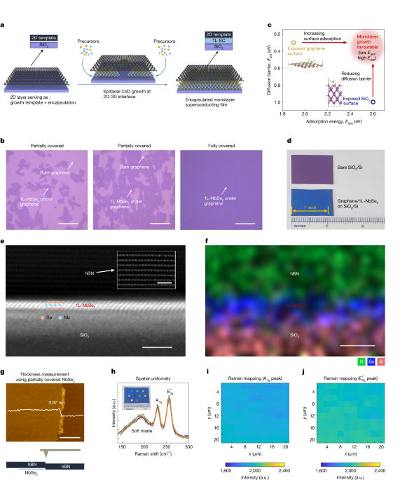
Saito, Y., Nojima, T. & Iwasa, Y. Highly crystalline 2D superconductors. Nat. Rev. Mater. 2, 16094 (2017).
Liu, X. & Hersam, M. C. 2D materials for quantum information science. Nat. Rev. Mater. 4, 669–684 (2019).
Wang, J. I. J. et al. Hexagonal boron nitride as a low-loss dielectric for superconducting quantum circuits and qubits. Nat. Mater. 21, 398–403 (2022).
Antony, A. et al. Miniaturizing transmon qubits using van der Waals materials. Nano Lett. 21, 10122–10126 (2021).
Balgley, J. et al. Crystalline superconductor–semiconductor Josephson junctions for compact superconducting qubits. Phys. Rev. Appl. 24, 034016 (2025).
Cao, Y. et al. Quality heterostructures from two-dimensional crystals unstable in air by their assembly in inert atmosphere. Nano Lett. 15, 4914–4921 (2015).
Xi, X. et al. Strongly enhanced charge-density-wave order in monolayer NbSe2. Nat. Nanotechnol. 10, 765–769 (2015).
Peri, V., Ilani, S., Lee, P. A. & Refael, G. Probing quantum spin liquids with a quantum twisting microscope. Phys. Rev. B 109, 035127 (2024).
Xi, X. et al. Ising pairing in superconducting NbSe2 atomic layers. Nat. Phys. 12, 139–143 (2016).
Li, T. et al. Epitaxial growth of wafer-scale molybdenum disulfide semiconductor single crystals on sapphire. Nat. Nanotechnol. 16, 1201–1207 (2021).
Zhu, J. et al. Low-thermal-budget synthesis of monolayer molybdenum disulfide for silicon back-end-of-line integration on a 200 mm platform. Nat. Nanotechnol. 18, 456–463 (2023).
Xia, Y. et al. 12-inch growth of uniform MoS2 monolayer for integrated circuit manufacture. Nat. Mater. 22, 1324–1331 (2023).
Zhou, J. et al. A library of atomically thin metal chalcogenides. Nature 556, 355–359 (2018).
Ugeda, M. M. et al. Characterization of collective ground states in single-layer NbSe2. Nat. Phys. 12, 92–97 (2016).
Naritsuka, M. et al. Superconductivity controlled by twist angle in monolayer NbSe2 on graphene. Nat. Phys. 21, 746–753 (2025).
Wang, H. et al. High-quality monolayer superconductor NbSe2 grown by chemical vapour deposition. Nat. Commun. 8, 394 (2017).
Li, J. et al. Printable two-dimensional superconducting monolayers. Nat. Mater. 20, 181–187 (2021).
Zhou, Z. J. et al. Stack growth of wafer-scale van der Waals superconductor heterostructures. Nature 621, 499–505 (2023).
Fu, Z. et al. Van der Waals growth of monolayer transition metal dichalcogenide superconductors on ultra-flat graphene. 2D Mater. 12, 015021 (2024).
Al Balushi, Z. et al. Two-dimensional gallium nitride realized via graphene encapsulation. Nat. Mater. 15, 1166–1171 (2016).
Pécz, B. et al. Indium nitride at the 2D limit. Adv. Mater. 33, 2006660 (2021).
Liu, X. & Hersam, M. C. Borophene–graphene heterostructures. Sci. Adv. 5, eaax6444 (2019).
Xie, C. et al. Space-confined growth of monolayer ReSe2 under a graphene layer on Au foils. Nano Res. 12, 149–157 (2019).
Bian, C. et al. Atomically precise synthesis and simultaneous heterostructure integration of 2D transition metal dichalcogenides through nano-confinement. Nat. Mater. https://doi.org/10.1038/s41563-026-02495-9 (2026).
Chen, C. W., Choe, J. & Morosan, E. Charge density waves in strongly correlated electron systems. Rep. Prog. Phys. 79, 084505 (2016).
Venables, J. A., Spiller, G. D. T. & Hanbucken, M. Nucleation and growth of thin films. Rep. Prog. Phys. 47, 399–459 (1984).
Venables, J. A. Atomic processes in crystal growth. Surf. Sci. 200–300, 798–817 (1994).
Seebauer, E. G. & Allen, C. E. Estimating surface diffusion coefficients. Prog. Surf. Sci. 49, 265–330 (1995).
Wickramaratne, D., Khmelevskyi, S., Agterberg, D. F. & Mazin, I. Ising superconductivity and magnetism in NbSe2. Phys. Rev. X 10, 041003 (2020).
Moon, D. et al. Hypotaxy of wafer-scale single-crystal transition metal dichalcogenides. Nature 638, 957–964 (2025).
Cho, K. et al. Using controlled disorder to probe the interplay between charge order and superconductivity in NbSe2. Nat. Commun. 9, 2796 (2018).
Lee, J. et al. Optical separation of mechanical strain from charge doping in graphene. Nat. Commun. 3, 1024 (2012).
Wang, Y. et al. Modulation doping via a two-dimensional atomic crystalline acceptor. Nano Lett. 20, 8446–8452 (2020).
Zheng, X. et al. Electrostatic-repulsion-based transfer of van der Waals materials. Nature 645, 906–914 (2025).
Tinkham, M. et al. Hysteretic I–V curves of superconducting nanowires. Phys. Rev. B 68, 134515 (2003).
Sinko, M. R. et al. Superconducting contact and quantum interference between two-dimensional van der Waals and three-dimensional conventional superconductors. Phys. Rev. Mater. 5, 014001 (2021).
Tanaka, M. et al. Superfluid stiffness of magic-angle twisted bilayer graphene. Nature 638, 99–105 (2025).
Zaman, S. et al. Kinetic inductance of few-layer NbSe2 in the two-dimensional limit. Nat. Commun. https://doi.org/10.1038/s41467-026-75672-8 (2026).
Probst, S., Song, F. B., Bushev, P. A., Ustinov, A. V. & Weides, M. Efficient and robust analysis of complex scattering data under noise in microwave resonators. Rev. Sci. Instrum. 86, 024706 (2015).
Frasca, S. et al. NbN films with high kinetic inductance for high-quality compact superconducting resonators. Phys. Rev. Appl. 20, 044021 (2023).
Bretz-Sullivan, T. M. et al. High kinetic inductance NbTiN superconducting transmission line resonators in the very thin film limit. Appl. Phys. Lett. 121, 052602 (2022).
Amin, K. R. et al. Loss mechanisms in TiN high impedance superconducting microwave circuits. Appl. Phys. Lett. 120, 164001 (2022).
Winkel, P. et al. Implementation of a transmon qubit using superconducting granular aluminum. Phys. Rev. X 10, 031032 (2020).
Niepce, D., Burnett, J. & Bylander, J. High kinetic inductance NbN nanowire superinductors. Phys. Rev. Appl. 11, 044014 (2019).
Shearrow, A. et al. Atomic layer deposition of titanium nitride for quantum circuits. Appl. Phys. Lett. 113, 212601 (2018).
Samkharadze, N. et al. High-kinetic-inductance superconducting nanowire resonators for circuit QED in a magnetic field. Phys. Rev. Appl. 5, 44004 (2016).
Coumou, P. C. J. J. et al. Microwave properties of superconducting atomic-layer deposited TiN films. IEEE Trans. Appl. Supercond. 23, 7500404–7500404 (2013).
Shaikhaidarov, R. S. et al. Quantized current steps due to the a.c. coherent quantum phase-slip effect. Nature 608, 45–49 (2022).
Szypryt, P. et al. Kinetic inductance current sensor for visible to near-infrared wavelength transition-edge sensor readout. Commun. Eng. 3, 160 (2024).
Rieger, D. et al. Granular aluminium nanojunction fluxonium qubit. Nat. Mater. 22, 194–199 (2023).
Xue, G. et al. Large-area epitaxial growth of transition metal dichalcogenides. Chem. Rev. 124, 9785–9865 (2024).
Kresse, G. & Furthmüller, J. Efficiency of ab-initio total energy calculations for metals and semiconductors using a plane-wave basis set. Comput. Mater. Sci. 6, 15–50 (1996).
Sheppard, D., Terrell, R. & Henkelman, G. Optimization methods for finding minimum energy paths. J. Chem. Phys. 128, 134106 (2008).
Redhead, P. A. Thermal desorption of gases. Vacuum 12, 203–211 (1962).
Frank Zhao, S. Y. et al. Time-reversal symmetry breaking superconductivity between twisted cuprate superconductors. Science 382, 1422–1427 (2023).
Senger, C. et al. Defect healing in graphene via rapid thermal annealing with polymeric “nanobandage”. Small 19, 2206295 (2023).
Sakuma, Y. et al. Self-aligned and self-limiting van der Waals epitaxy of monolayer MoS2 for scalable 2D electronics. Nat. Commun. 17, 602 (2026).
Jain, A. et al. Commentary: The Materials Project: a materials genome approach to accelerating materials innovation. APL Mater. 1, 011002 (2013).
Grünhaupt, L. et al. Granular aluminium as a superconducting material for high-impedance quantum circuits. Nat. Mater. 18, 816–819 (2019).
Moshe, A. G., Farber, E. & Deutscher, G. Granular superconductors for high kinetic inductance and low loss quantum devices. Appl. Phys. Lett. 117, 062601 (2020).
Khestanova, E. et al. Unusual suppression of the superconducting energy gap and critical temperature in atomically thin NbSe2. Nano Lett. 18, 2623–2629 (2018).
Zhang, Y. et al. Edge-epitaxial growth of 2D NbS2–WS2 lateral metal–semiconductor heterostructures. Adv. Mater. 30, 1803665 (2018).
Su, J. et al. Sub-millimeter-scale monolayer p-type H-phase VS2. Adv. Funct. Mater. 30, 2000240 (2020).
You, J. et al. Salt-assisted selective growth of H-phase monolayer VSe2 with apparent hole transport behavior. Nano Lett. 22, 10167–10175 (2022).
Jiang, Y. C., Gao, J. & Wang, L. Raman fingerprint for semi-metal WTe2 evolving from bulk to monolayer. Sci. Rep. 6, 19624 (2016).

