With the distinct advantages of overcoming the bandwidth, noise figure and wavelength range of a stimulated-emission optical amplifier and generating waves beyond those achievable with conventional lasers, four-wave mixing (FWM) has led to numerous applications in various fields. In particular, hyper-dispersion engineering (second- and fourth-order dispersion in tandem) is very critical for broadband FWM with parametric gain, which is being pursued in various areas, such as ultra-long-haul transmission11, all-optical high-speed signal processing12, light detection and ranging13, and biochemistry analysis14. Since the invention of low-loss silica fibres, which offer long nonlinear optical interaction distances, fibre-based FWM has been intensively investigated15. However, the fibres exhibit low nonlinearity as well as a narrow parametric bandwidth and suffer from polarization and dispersion drifts, which reduce both FWM efficiency and bandwidth16. Because of their high nonlinearity, small footprint and flexible patterning, χ(3)-based nonlinear integrated waveguides provide excellent on-chip control of the optical field properties, such as dispersion and polarization state, potentially paving the way to high-efficiency and wideband FWM17. Nonlinear semiconductor integrated waveguides with a low refractive index contrast formerly attracted much interest for use in FWM but suffer from limited dispersion engineering and severe interference from other nonlinear effects18. Advances in deposition and bonding have enabled the creation of high-refractive-index-contrast nonlinear integrated waveguide structures with silica cladding that offer strong field confinement and dispersion engineering19 and are ideally suited for broadband parametric signal processing. Many kinds of such nonlinear platforms have been explored, including silicon6,20,21, silicon nitride22,23,24, aluminium gallium arsenide7,25,26, nonlinear glasses9,10 and graphene27. In particular, a continuous-wave optical parametric gain due to FWM was achieved for the first time recently in nonlinear Si3N4 integrated waveguides, due to a balance of propagation loss, nonlinearity, power handling ability and dispersion engineering22, which also corresponds to high conversion efficiencies (the power ratio of the output idler to input signal).
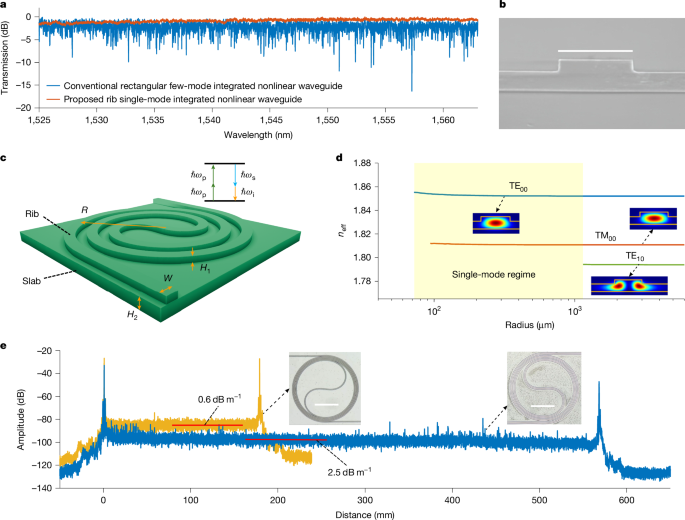
For pump-degenerate FWM, a strong pump wave (p) and a weak signal wave (s) were passed into a χ(3)-based nonlinear optical medium, where the signal was amplified and an idler wave was generated at an angular frequency of ωi = 2ωp − ωs, as illustrated in Fig. 1c. The phase mismatch parameter \(\Delta K={\sum }_{k=1}^{\infty }2{\beta }_{2k}{\Delta \omega }^{2k}/(2k)\,!+2\gamma P\) affects the gain, conversion efficiency and bandwidth. Here βi is the ith-order derivative with respect to the angular frequency ω of the optical propagation constant β evaluated at the pump frequency, γ is the nonlinear coefficient, Δω is the angular frequency difference between the pump and signal waves and P is the pump power28. Anomalous dispersion (β2 < 0) is of vital importance for realizing phase matching (ΔK = 0) for high parametric gain and wide bandwidth, as can be seen in the Supplementary Information. However, conventional high-index-contrast silica-clad nonlinear integrated waveguides are multi-mode to achieve anomalous dispersion6,7,10,22,23, but the focus has only been on the transverse cross-sectional geometry of the waveguide. Consequently, random and unavoidable modal coupling results in power drops for both the signal and pump waves, which not only decreases the FWM gain, conversion efficiency and bandwidth but also distorts the modulated signals29. For instance, the blue curve in Fig. 1a is the measured normalized transmission spectrum of a conventional rectangular-core dispersion-engineered nonlinear Si3N4 integrated waveguide whose fabrication was optimized to reduce the sidewall roughness. This waveguide was 2,000 nm wide, 690 nm high and about 50 cm long and supported four modes in transverse electric polarization. As can be seen in Fig. 1a, this typical conventional nonlinear Si3N4 integrated waveguide suffers from serious spectral fluctuations (power fading at some wavelengths of more than 10 dB) due to random mode coupling. Single-mode χ(3)-based high-index-contrast silica-clad nonlinear integrated waveguides with simultaneous anomalous dispersion are in great need for FWM but have not been reported so far. Moreover, hyper-dispersion engineering (β4 in tandem with β2) is quite important for ultimately broadening the FWM bandwidth. Nevertheless, ultra-broadband FWM with high conversion efficiency assisted by hyper-dispersion engineering in single-mode nonlinear waveguides has not yet been demonstrated.
a, Normalized measured transmission spectra of a conventional rectangular-core (blue) and a proposed single-mode rib (red) nonlinear Si3N4 integrated waveguide. The fabrication of the few-mode rectangular-core nonlinear spiral Si3N4 integrated waveguide was optimized to reduce sidewall roughness. The wavelength tuning step in the measurements was 1 pm. Both waveguides were about 50 cm long. b, Scanning electron microscope image of the cross section of one proposed single-mode nonlinear rib Si3N4 integrated waveguide. c, Schematic diagram of one unit of the proposed spiral single-mode dispersion-engineered rib nonlinear integrated waveguide. The maximum bend radius in the spiral area was controlled to simultaneously achieve single-mode operation and anomalous dispersion. Several spiral units were concatenated to generate a metres-long nonlinear integrated waveguide. The cladding was SiO2. d, Effective refractive index (neff) of different modes in a nonlinear rib Si3N4 integrated waveguide versus the bend radius, with W = 1.9 μm, H1 = 300 nm and H2 = 500 nm. The blue, red and green lines are for the TE00, TM00 and TE10 modes, respectively. Insets, intensity profiles of the different modes. The yellow lines are the SiO2–Si3N4 boundaries. e, OFDR traces of 18-cm-long (yellow, WG1) and 56-cm-long (blue, WG2) single-mode nonlinear rib Si3N4 integrated waveguides when the wavelength was scanned from 1,480 nm to 1,640 nm. The minimal propagation losses of WG1 and WG2 were 0.6 dB m−1 and 2.5 dB m−1 (red lines). Insets, optical microscope images of one spiral unit of WG1 and WG2 on two wafers, respectively. Scale bars, 1.9 μm (b), 0.3 mm (e).
We propose a universal design method for achieving anomalous-dispersion single-mode nonlinear integrated waveguides to address the above issues. The method combines longitudinal bending with a transverse cross-sectional construction. The red curve in Fig. 1a is the measured transmission spectrum of one waveguide that we designed and fabricated (Methods). It has an excellent single-mode property in contrast to the conventional rectangular-core nonlinear integrated waveguide. Rib waveguides with silica cladding are used to achieve fewer guiding modes and lower propagation losses compared to rectangular-core waveguides with the same width and total thickness19,30,31.
Figure 1b is a scanning electron microscope image of the cross section of a proposed 1.9-μm-wide single-mode nonlinear rib Si3N4 integrated waveguide. The key technique for simultaneously achieving single-mode operation and anomalous dispersion is to bend the waveguide to cut off higher-order modes and maintain the anomalous dispersion. Figure 1c is a schematic diagram of the proposed waveguide. W, R, H1 and H2 are the rib width, radius, height and slab thickness, respectively. To verify the proposed method, we used the Si3N4 integrated platform as an example to realize single-mode dispersion-engineered nonlinear waveguides for parametric gain. Figure 1d presents the simulated effective refractive index (neff) of different modes as a function of waveguide radius at wavelength 1,550 nm. In the simulation, the nonlinear rib Si3N4 waveguide was 1.9 μm wide with H1 = 300 nm and H2 = 500 nm. The blue and red lines correspond to the fundamental transverse-electric and transverse-magnetic modes. As can be seen in Fig. 1d, when it is straight, this nonlinear rib Si3N4 waveguide supports three modes. When the radius was reduced to less than 1,150 μm, the high-order mode TE10 (green line) was cut off. Hence, with the right bend arrangement, we obtained a nonlinear spiral-rib Si3N4 waveguide with a single mode per polarization. Extended Data Fig. 1 presents the simulated effective refractive index versus wavelength. The cutoff wavelength of the TE10 mode was 1,180 nm for a bending radius of 400 μm. We show in the Supplementary Information how the propagation of the TE00 and TE10 modes was affected by bending. With a larger nonlinear coefficient than the TM00 mode, we used the TE00 mode for FWM. The TE00 mode dispersion at 1,550 nm could become anomalous and tuned by changing the waveguide width and radius (Extended Data Fig. 2a,b).
For the fabrication tolerance analysis, Extended Data Fig. 2c,d presents the second- and fourth-order dispersion for small rib dimensions. Moreover, Fig. 1e shows the traces of optical frequency-domain reflectometry (OFDR) of two TE00-mode-coupled 1.9-μm-wide nonlinear spiral-rib Si3N4 integrated waveguides with lengths of 18 cm (yellow, WG1) and 56 cm (blue, WG2). The slab widths of WG1 and WG2 were sufficiently large such that the TE00 mode was not affected by the slab sidewall and did not couple to adjacent rib waveguides (Supplementary Information). The red line in Fig. 1e indicates that the measured propagation loss of WG1 was 0.6 dB m−1. For WG2, the propagation loss was about 2.5 dB m−1. The insets in Fig. 1e are optical microscope images of WG1 and WG2, respectively. One can see that WG2 suffered from residual nanoparticles of which WG1 was almost free. The propagation loss difference between WG1 and WG2 was mainly due to fabrication variation, which we are trying to improve. We fabricated six 56-cm-long single-mode nonlinear rib Si3N4 integrated waveguides. WG2 was the only one without large defects on the OFDR traces. The yield for the 18-cm-long rib waveguides was 4/20, which was mainly limited by the misalignment of the dual-layer tapers and minor defects.
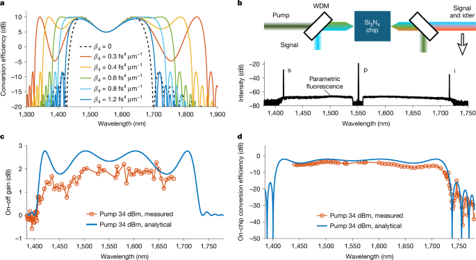
Apart from the single-mode waveguiding property, we investigated how the hyper-dispersion engineering ultimately extended the bandwidth of the FWM-based parametric process. Figure 2a depicts the theoretical conversion-efficiency spectra of a 1-m-long nonlinear integrated waveguide with a pump power of 35 dBm at 1,550 nm. In the calculation, the second-order dispersion was −1 ps2 km−1 at 1,550 nm, the effective nonlinear coefficient was 0.7 W−1 m−1 and the waveguide loss was 1 dB m−1. The maximum conversion efficiency was 10 dB, which corresponds to a maximum parametric gain of about 10 dB for the signal wave32. The parametric gain spectrum was like the spectral curve for conversion efficiency in this case. The black dashed line is for β4 = 0 for which the amplification bandwidth was 270 nm. The red, yellow, green and blue solid lines are for β4 = 0.3, 0.4, 0.6 and 1.2 fs4 μm−1, respectively. As shown by Fig. 2a, the amplification bandwidth increased to 542 nm for β4 = 0.3 fs4 μm−1, as the fourth-order dispersion led to new phase-matching wavelengths28. When the balance among the nonlinear shift, second- and fourth-order dispersion was achieved with β4 = 0.6 fs4 μm−1, two flat gain regimes were obtained. The amplification bandwidth reached 385 nm (43% bandwidth increase compared to β4 = 0). Hence, fourth-order dispersion plays a vital role in realizing ultra-wideband parametric devices.
a, Theoretical conversion-efficiency spectral curves of 1-m-long χ(3)-base nonlinear integrated waveguides with various fourth-order dispersions. The waveguide loss was 1 dB m−1, the nonlinear coefficient was 0.7 W−1 m−1 and the second-order dispersion was −1 ps2 km−1. The power at 1,550 nm wavelength was 35 dBm. The red, yellow, green, light blue and dark blue solid lines are for β4 = 0.3, 0.4, 0.6, 0.8 and 1.2 fs4 μm−1, respectively. The black dashed line corresponds to the case where fourth-order dispersion is not considered. b, Top, experimental set-up for the FWM characterization of the 0.56-m-long single-mode nonlinear rib Si3N4 integrated waveguide. Bottom, spectrum after the WDM coupler with a 1,551.1 nm pump and a 1,415 nm signal. c,d, Measured (red circles) on–off parametric gain (c) and on-chip conversion efficiency (d) of the single-mode nonlinear Si3N4 integrated waveguide with a 34-dBm on-chip pump power. The solid blue curves were calculated analytically with the assumption of a spectrally constant waveguide loss of 2.5 dB m−1.
Furthermore, we characterized the ultra-broadband FWM in WG2 using continuous-wave pump–probe approaches based on the experimental diagram in Fig. 2b (Methods). The on-chip pump power was 34 dBm considering the coupling loss. The lower part of Fig. 2b shows the output optical spectrum of WG2 with the residual pump mitigated by a wavelength-division multiplexing (WDM) coupler. The signal, pump and idler wavelengths were 1,415, 1,551.1 and 1,716 nm, respectively. Ultra-wideband flat parametric fluorescence during FWM was also observed, as can been seen in Fig. 2b. Figure 2c,d depicts the measured (blue) on–off parametric gain and on-chip conversion-efficiency spectra, respectively. The on–off gain was used as it can mitigate the impact of the wavelength-dependent coupling loss of the tapers on the measurements. The solid lines are theoretically fitted spectra with β2 = −2.2 ps2 km−1 and β4 = 1.9 fs4 μm−1 at 1,551 nm. The measured and theoretical curves are in good agreement with small discrepancies, which may be due to the wavelength-dependent loss of the waveguide. The on-chip waveguide loss in the L band was about 1 dB, indicating that we achieved an on-chip net continuous-wave parametric gain of 1 dB. Besides, we obtained a maximum on-chip conversion efficiency of −3.4 dB at 1,500-nm wavelength, as shown in Fig. 2d. The gain and conversion-efficiency spectra in Fig. 2c,d indicate that we realized a FWM bandwidth of 330 nm—one of the widest bandwidths of all reported continuous-wave optical amplifiers to date. As there were not enough lasers to cover the full FWM bandwidth during the measurements, we recorded the pure parametric-fluorescence spectrum as a measure of the parametric gain profile, which changed with the dispersion by adjusting the pump wavelength (Supplementary Information). Moreover, the fitted second- and fourth-order dispersion agreed with the waveguide design, as we can see from Extended Data Fig. 2c,d, which verifies that the nonlinear Si3N4 integrated platform is very tolerant to fabrication uncertainties. β2 was more sensitive to variations in the thickness, whereas β4 exhibited a larger tolerance to dimension variations, as can be seen from Extended Data Fig. 2c,d. The fitted β2 is slightly smaller than the designed value of −4 ps2 km−1, which is mainly attributed to the thickness variation of the waveguide. Si3N4 wafers will be planarized to improve the thickness uniformity33.
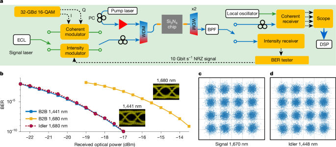
Furthermore, we applied the Si3N4-chip ultra-broadband efficient FWM to all-optical high-speed wavelength conversion for communications. Figure 3a shows the experimental set-up with intensity and coherent modulation (Methods). We used 10 Gbit s−1 non-return-to-zero (NRZ) intensity modulation to check the impairments to the idler quality during wavelength conversion. Figure 3b presents the bit-error rate (BER) of the back-to-back (B2B) 1,441 nm signal (blue solid line), 1,680 nm signal (yellow solid line) and 1,441 nm idler (purple dotted line). The B2B BER difference between 1,441 and 1,680 nm signals was due to the wavelength-dependent responsivity of the intensity receiver. As can be seen in Fig. 3b, the idler suffered negligible penalty compared to the 1,441 nm B2B signal, which indicates that the proposed CMOS-compatible single-mode nonlinear Si3N4 integrated waveguide is promising for all-optical signal processing. In addition, we implemented the all-optical wavelength conversion of single-polarization 32-GBd 16-quadrature-amplitude-modulation (16-QAM) signals with a net rate over 100 Gbit s−1, based on the 56-cm-long single-mode nonlinear Si3N4 integrated waveguide. Figure 3c,d show the constellation diagrams for the B2B 1,670-nm signal and converted 1,448-nm idler, respectively. We have realized all-optical wavelength conversion for a more than 200-nm-wide wavelength span at 100 Gbit s−1 without amplifying the signal and idler waves. As the 32-GBd 16-QAM is the dominant modulation format of current optical-fibre communication systems connecting the continents on Earth, the Si3N4-chip high-efficiency wavelength conversion demonstrated has a bright future in the all-optical reconfiguration of global WDM optical networks by unlocking transmission beyond the C and L bands of optical fibres34 and increasing the capacity of optical neuromorphic computing for artificial intelligence35.
a, Experimental set-up of the Si3N4-chip-based all-optical wavelength conversion for both intensity modulation and coherent optical communications. The on-chip pump power was 34 dBm. b, BER as a function of received optical power of 10 Gbit s−1 NRZ signals (1,680 nm) and converted idlers (1,441 nm, purple dashed line). Insets, eye diagrams of the B2B optical signals at wavelengths of 1,441 nm and 1,680 nm, respectively. c,d, Constellation diagrams for a 1,670-nm signal (c) and a 1,448-nm idler (d) with 32-GBd 16-QAM after offline digital signal processing (DSP). BPF, band-pass filter; PC, polarization controller.
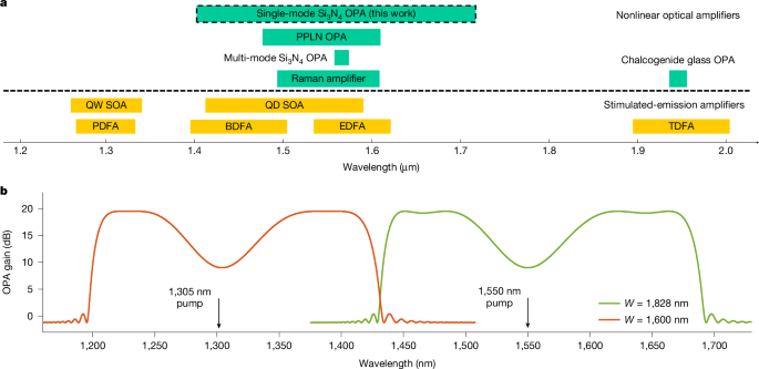
Figure 4a summarizes the bandwidth of various types of wideband continuous-wave optical amplifiers. Various material platforms have been developed for stimulated-emission optical amplifiers, such as erbium-doped fibre amplifiers36, bismuth-doped fibre amplifiers37, thulium-doped fibre amplifiers for optical applications38, praseodymium-doped fibre amplifiers39, and quantum-well and quantum-dot semiconductor optical amplifiers40,41. To cover the entire transmission windows of telecommunication-grade silica and widely studied hollow-core fibres42, new stimulated-emission materials with different bandgaps need to be investigated and developed. On the other hand, nonlinear optical effects, including the Raman effect43, difference-frequency generation and FWM, have also been applied to build wideband optical amplifiers based on single material such that the operating wavelength can be flexibly tuned by changing the pump frequency and the waveguide dispersion. Amplifiers based on the difference-frequency or FWM effects are also called optical parametric amplifiers (OPAs). Periodically poled lithium niobate waveguide OPAs based on the difference-frequency effect have been investigated44, leading to ultra-high-speed optical-fibre transmission beyond conventional telecommunication bands45. Based on the FWM process, OPAs using χ(3)-nonlinear nanophotonic waveguides are free of complicated periodic poling. Continuous-wave nanophotonic OPAs were first realized with chalcogenide glass microfibres with a gain bandwidth of about 20 nm (ref. 46). Our single-mode nonlinear rib χ(3) integrated waveguides, which have more freedom in dispersion engineering, enabled us to demonstrate an OPA bandwidth of 330 nm (Fig. 4a), which is wider than that of previously published continuous-wave optical amplifiers. At present, the length of the fabricated 1.9-μm-wide single-mode nonlinear spiral-rib Si3N4 integrated waveguide greatly limits the parametric gain. We are continuing to optimize the fabrication and believe that the yield of long ultra-low-loss single-mode nonlinear rib Si3N4 waveguides can be improved. The length issue together with the yield may not be problematic for CMOS foundries, as their deep-ultraviolet exposure technologies are mature for massive nanofabrication.
a, State-of-the-art bandwidth of continuous-wave optical amplification in the near-infrared regime based on both stimulated-emission and nonlinear optical platforms. b, Theoretical gain spectra of OPAs based on optimized single-mode nonlinear rib Si3N4 integrated waveguides pumped at wavelengths of 1,305 nm (red) or 1,550 nm (green). Both Si3N4 waveguides have the same rib and slab thicknesses (H1 = 300 nm and H2 = 500 nm) and can be integrated on the same wafer but for different widths of 1,600 nm and 1,828 nm. The waveguide lengths are 2 m with an assumed propagation loss of 0.6 dB m−1. BDFA, bismuth-doped fibre amplifier; EDFA, erbium-doped fibre amplifier; PDFA, praseodymium-doped fibre amplifier; PPLN, periodically poled lithium niobate; QD, quantum dot; QW, quantum well; SOA, semiconductor optical amplifier; TDFA, thulium-doped fibre amplifier.
We theoretically optimized the width of the single-mode nonlinear rib Si3N4 integrated waveguide for high-gain OPAs. Figure 4b shows the theoretical parametric gain spectra of 2-m-long 0.6 dB m−1-loss single-mode nonlinear rib Si3N4 integrated waveguides with widths of 1,600 nm (red) and 1,828 nm (green) and a pump power of 34 dBm. Both waveguides have the same rib thickness (H1 = 300 nm) and slab thickness (H2 = 500 nm) and can be integrated on the same wafer, potentially with a total chip size of 3 cm × 3 cm. As can be seen in Fig. 4b, the two OPAs, for which the pump wavelengths are 1,305 and 1,550 nm, provide a maximum gain of about 20 dB and cover the whole transmission window of single-mode telecommunication fibres. We also analysed the fabrication tolerance of the high-gain Si3N4 waveguide OPA (Supplementary Information). With the advances in semiconductor optoelectronics, continuous-wave pump lasers operating at wavelengths of 1,305 and 1,550 nm with watt-level power could also become available47 and may lead to compact OPAs based on hybrid photonic integration48. The spectral flatness of the OPA over the 200-nm bandwidth could be improved by dual-pump, dispersion or pump-phase shifting techniques that can be implemented in integrated waveguide platforms49,50. A rib structure with several layers would provide more degrees of freedom for hyper-dispersion engineering and may lead to a broader parametric bandwidth, which is yet to be explored.
In this paper, we proposed and demonstrated extremely low-loss single-mode nonlinear Si3N4 integrated waveguides with hyper-dispersion engineering for ultra-broadband, efficient, continuous-wave FWM. Unlike conventional approaches focusing on the waveguide cross section, we exploited the three-dimensional waveguide geometry for on-chip optical field manipulation, simultaneously achieving single-mode transmission and dispersion engineering of nonlinear integrated nanophotonic waveguides in telecommunication bands. Using the 0.56-m-long single-mode nonlinear rib Si3N4 integrated waveguide with hyper-dispersion engineering, we obtained a continuous-wave gain bandwidth of 330 nm in the near-infrared regime. The whole transmission window of telecommunication silica fibres could potentially be covered by the parametric gain profiles of single-mode nonlinear rib Si3N4 waveguides integrated on the same wafer. Furthermore, we realized wide all-optical wavelength conversion of single-wavelength signals beyond 100 Gbit s−1 without amplifying the signal and idler wave. These experimental results agree with theoretical expectations. A higher continuous-wave parametric gain and conversion efficiency could be expected with longer low-loss single-mode nonlinear rib Si3N4 integrated waveguides. With the combination of cross-sectional shaping and longitudinal bending, the waveguide design technique we proposed is easy to implement. It could allow other integrated platforms to realize low-loss single-mode dispersion-engineered nonlinear waveguides that could become key building blocks for optics, making the technique promising, from fundamental research in photonics, physics, quantum physics, chemistry and biology to industrial applications in communications, computing, spectroscopy, imaging and metrology.


