Device fabrication
The bottom control gates (5/15 nm Cr/Au) were patterned by e-beam lithography with a bilayer photoresist process followed by deposition of metal by e-beam evaporation on silicon dioxide (300 nm)/silicon substrates. For the flash memory, following the preparation of the bottom gates, an Al2O3 blocking oxide and an HfO2 trap layer were grown by thermal atomic-layer deposition at 250 °C. During the atomic-layer-deposition process, trimethylaluminium and tetrakis(ethylmethylamino)hafnium reacted with water to form Al2O3 and HfO2, respectively. This atomic-layer-deposition process is necessary only for flash fabrication. WSe2, graphene and hBN bulk crystals were purchased from HQ Graphene and the heterostructure of the 2D materials was prepared using mechanical exfoliation and a dry-transfer approach. The hBN flake was first transferred to the bottom gate, and then the thin-body material was transferred onto the hBN flake. The adhesion of the heterostructure on the substrate was improved by heat annealing for more than 2 h at 200 °C under a nitrogen atmosphere. Next, drain–source contacts were patterned by e-beam lithography, and a metal stack (WSe2, 10/12 nm Sb/Pt; graphene, 5/60 nm Cr/Au stack) was deposited using e-beam evaporation. After the standard lift-off approach, devices with the Sb/Pt contact were annealed by the hot plate in the glove box (200 °C, 2 h) to form the alloy. To conduct the sub-1-ns flash memory test, metal wires and pads matched with the radio-frequency probes were patterned by e-beam lithography, and 5/60 nm Cr/Au was deposited by e-beam evaporation.
Material characterization
Atomic force microscopy for the devices was measured by a MFP-3D Origin+ (Asylum Research, Oxford Instruments) system. The transmission-electron-microscopy-ready sample was prepared using an in situ focused ion-beam lift-out technique on a Thermo Scientific Helios Eurofins EAG lab G4 HX or UC Dual Beam focused ion-beam/scanning electron microscope. The sample was plated with iridium and capped with electron-beam Pt and ion-beam Pt before milling. The transmission electron microscopy image was captured with a Thermo Scientific Tecnai F20 transmission electron microscope operated at an accelerating voltage of 200 kV. Energy-dispersive spectroscopy was performed on the Super X FEI System under scanning transmission electron microscopy mode.
Electrical measurements
In this work, the devices were measured at room temperature and under atmospheric conditions in a probe station (MPI, TS200-SE). The 2D-HCI mechanism verification under various temperatures was performed using a Lake Shore vacuum low-temperature probe station under a vacuum of <10−4 mbar. The d.c. signals were generated using a source measure unit (B1500A, Keysight). The voltage pulses (≥20 ns) were generated using a semiconductor pulse generator unit (B1500A, Keysight). The sub-1-ns measurement was conducted based on our homemade high-speed system (Supplementary Fig. 19). The waveforms of the voltage pulse were captured by the oscilloscope (DPO 5204, Tektronix). The electrical test was conducted using a semiconductor device parameter analyser (B1500A, Keysight).
Theoretical derivation of quasi-2D model
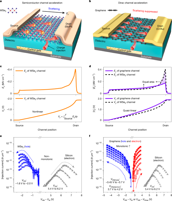
We employed a quasi-2D model with the same structure as our fabricated 2D transistor for analysis. The x direction is defined as the channel surface to gate vertically, and the y direction is defined as source to drain horizontally, where the zero point of the x and y axes is the channel surface and source, respectively. y0 is at the leading edge of the velocity saturation region, V(y) is the horizontal potential in the channel, tch is the channel thickness, Ex and Ey are the vertical and horizontal electric field in the channel, Edielectric is the vertical electric field in the dielectric, and Esat and VDSsat are the Ey and V(y) at the leading edge of the velocity saturation region, respectively. To obtain the Ey distribution, it is necessary to solve Poisson’s equation and the current transport equation simultaneously in the velocity saturation region. It is expressed as
$$\frac\partial ^2V(x,y)\partial x^2+\frac\partial ^2V(x,y)\partial y^2=\frac\rho (x,y)\varepsilon _\varepsilon _\rmch$$
(4)
where ρ(x, y) is the charge enclosed in the Gaussian box, ε0 is the vacuum permittivity and εch is the channel relative permittivity. Under the conditions of (1) the thin body (tch → 0) of the 2D material channel results in a square pinch-off region, denoted as a Gaussian box, (2) Ey only varies with horizontal position, and (3) the value of Ex at x = 0 is close to zero, which allows us to replace \(\frac\partial E_x\partial x\) with the average value given by \(\fracE_x(t_\rmch,y)t_\rmch\), we apply Gauss’ law
$$-E_\rmsatt_\rmch+E_y(\,y)t_\rmch+\frac\varepsilon _\rmdielectric\varepsilon _\rmch\int _y_^yE_\rmdielectric(t_\rmch,k)\rmdk=\frac\rho (x,y)\varepsilon _\varepsilon _\rmcht_\rmch(\,y-y_)$$
(5)
where Edielectric is the electric field in the gate dielectric and εdielectric is the dielectric relative permittivity. Differentiating equation (5) with respect to y, we have
$$t_\rmch\frac\rmdE_y(y)\rmdy+\frac\varepsilon _\rmdielectric\varepsilon _\rmchE_\rmdielectric(t_\rmch,y)=\frac\rho (x,y)\varepsilon _\varepsilon _\rmcht_\rmch$$
(6)
We can express Edielectric(tch, y) as
$$E_\rmdielectric(t_\rmch,y)=\frac[V_\rmGS-V_\rmFB-2\varphi _\rmB-V(\,y)]t_\rmdielectric$$
(7)
where VGS is the gate–source bias, VFB is the flat-band voltage, φB is the surface potential and tdielectric is the dielectric thickness. As the boundary conditions at the leading edge of the Gaussian box: V(y = y0) = VDSsat and Edielectric(y = y0) = [VGS − VFB − 2φB − VDSsat]/tdielectric, we can obtain that \(\rho (x,y)=\frac\varepsilon _\varepsilon _\rmdielectrict_\rmcht_\rmdielectric(V_\rmGS-V_\rmFB-2\varphi _\rmB-V_\rmDSsat)\). Then equation (6) is simplified to
$$\frac\rmdE_y(\,y)\rmdy=\fracV(\,y)-V_\rmDSsat\lambda ^2,\,\textwhere\,\lambda ^2=\frac\varepsilon _\rmcht_\rmdielectrict_\rmch\varepsilon _\rmdielectric$$
(8)
where λ is the effective length of the Gaussian box, also known as the scale length. By applying the boundary conditions at the leading edge of the Gaussian box: V(y = y0) = VDSsat, and Ey(y = y0) = Esat, we can write the V(y) and Ey(y) in the Gaussian box as
$$V(y)=V_\rmDSsat+\lambda E_\rmsat\,\sinh \left(\fracy-y_\lambda \right)$$
(9)
and
$$E_y(y)=E_\rmsat\,\cosh \left(\fracy-y_\lambda \right)$$
(10)
At the drain end of the channel where the field peaks
$$E_y,\rm\textmax=E_y(\,y=y_+\Delta L)=E_\rm\textsat\,\cosh \left(\frac\Delta L\lambda \right)$$
(11)
and
$$V_\rmDSmax=V_\rmDSsat+\lambda E_\rmsat\,\sinh \left(\frac\Delta L\lambda \right)$$
(12)
where ΔL is the region that extends from the channel pinch-off point to the drain. Equations (11) and (12) can be combined to yield
$$\Delta L=\lambda \rm\textln\frac{\left\{\frac{[V_\rm\textDS-V_\rm\textDSsat]}\lambda \right\}+E_y,\rm\textmax}E_\rm\textsat$$
(13)
and
$$| E_y,\rm\textmax| =\sqrt{\frac{(V_\rmDS-V_\rmDSsat)^2}t_\rm\textch\frac\varepsilon _\rm\textdielectric\varepsilon _\rm\textcht_\rm\textdielectric+E_\rm\textsat^2}$$
(14)
This equation shows that the Ey,max is highly sensitive to tch scaling.


