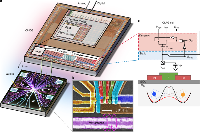
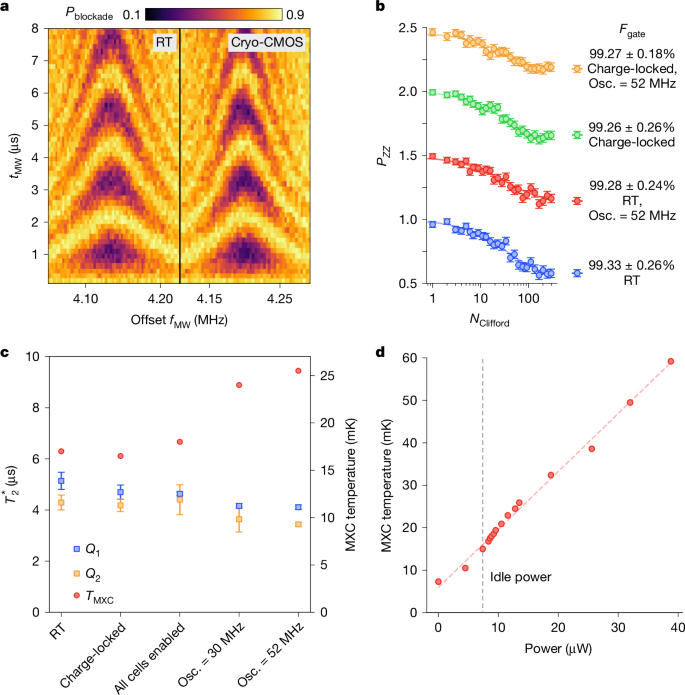
To evaluate single-qubit gates, we first establish a baseline using all room-temperature electronics for control. Following the usual protocol for two-spin manipulation1,24,25, the singlet state is first prepared in the (1, 3) charge configuration using pulses applied to detuning gates P1 and P2, with (n, m) labelling the number of electrons in each dot under P1 and P2, respectively. A pulse applied to the J gate, connected to Vhold, then increases the barrier, separating the two electrons into each dot, in which they are independently addressed using the microwave antenna through their unique resonance frequency (fESR = 13.9 GHz for a field B0 = 0.5 T). Free-induction decay (FID) of the target spin is produced by applying microwave power to the on-chip electron spin resonance (ESR) line. Finally, a second pulse of the J gate returns the spins to the readout configuration, in which Pauli spin blockade enables spin-to-charge conversion26,27 and measurement by the RF-SET. The shot-averaged readout signal as a function of microwave pulse time and frequency is shown in Fig. 2a. Beyond FID, we further establish our room temperature baseline by performing pulse sequences implementing Hahn echo (to measure coherence time T2; Extended Data Fig. 4) and randomized benchmarking (to measure qubit control fidelity)28,29. We have intentionally limited the number of qubit gates bonded to the CMOS control chip to facilitate direct comparison with room temperature control in the same cooldown. The present prototype CMOS chip contains 32 CLFG cells to drive 32 qubit gate electrodes.
a, Single-qubit Rabi oscillations (Q1) as a function of microwave (MW) frequency fMW and pulse time tMW, performed with room temperature (RT) control. b, Single-qubit randomized benchmarking (Q1) under various cryo-CMOS conditions. Traces are offset for clarity. Each data point is the average of 300 randomized sequences at 100 shots each. c, Single-qubit \(T_2^* \) coherence time as a function of select cryo-CMOS parameters. Unless otherwise indicated, all data use cryo-CMOS control. Each data point is the average of 100 shots with 4 repeats for a total of 400 single shots. d, Mixing chamber temperature with cryo-CMOS power. Error bars represent the 95% confidence level. Osc., oscillator.
In this single-qubit measurement, the function of the J-gate pulse is to separate the two-spin system for controlled rotation by spin resonance. As such, electrical noise, coupled through the J gate or other means, is unlikely to affect qubit fidelity in the limit that the pulse amplitude and duration are sufficiently large to fully separate the spins. Even so, we now evaluate the impact of cryo-CMOS control on single-qubit performance by performing the same protocol outlined above, but now with charge-locking applied to the J gate and the pulse produced using a CLFG cell under control of the FSM. Again, we generate FID data and quantitatively compare the CMOS and room temperature control using randomized benchmarking protocols, as shown in Fig. 2b. A slight degradation in qubit fidelity is observed (0.07%), probably because of unmitigated heat from the CMOS. We discuss heating in detail below.
Although electrical noise at the J gate does not directly couple with single spins, heat and drift in gate potential over longer timescales can affect qubit performance. Gate noise can also produce d.c. Stark shift of the qubit frequency in certain regimes (discussed further below). To investigate these mechanisms, we extract the time-ensemble average coherence time \(T_2^* \) for each qubit, repeatedly measured as each circuit block of the CMOS chip is powered up. Comparing the data in Fig. 2c again shows a small impact with respect to our room temperature baseline, correlating with a slight rise in the base temperature of the refrigerator (see Fig. 2d and its caption for details).
A drawback of the control scheme outlined above is its reliance on qubit-specific microwave pulses, which, despite cryo-CMOS gate control, require additional room-temperature microwave generators (and cables) for each qubit. We next demonstrate an alternate control approach that leverages a continuous wave global microwave field, sourced from room temperature but common to all qubits15,30. Key to this scheme is the ability to tune the spin resonance frequency of a qubit using a gate voltage31,32. This d.c. Stark shift enables a gate pulse to bring a qubit into resonance with the global field for a controlled amount of time to produce a rotation in the qubit state vector. With a single microwave tone from room temperature, cryo-CMOS produces the ‘baseband’ gate pulses that independently bring each qubit into and out of resonance with the global field.
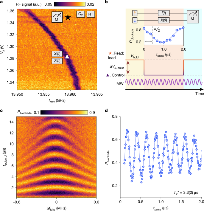
The global microwave scheme requires a calibration of the unique d.c.-Stark shift produced by the J gate on, for example, qubit Q2, as shown in Fig. 3a. The sizable shift (about 1 MHz per 10 mV) is well-matched to the voltage pulses that can be efficiently generated with proximal low-power CMOS. Here, the spins are initialized to a mixed or T− (|↓↓⟩) state off-resonance by a detuning pulse to a relaxation hot-spot33,34. The J-gate pulse produces the time-controlled Stark shift as shown in Fig. 3b. Repeating this sequence as a function of pulse length yields the coherent oscillations (Fig. 3c), and coherence metrics can be extracted (Fig. 3d). For this measurement, the width of the pulse is set by the timing of the trigger fed to the CMOS from room temperature. Conceptually, this reliance on room temperature triggering may seem to be a limitation of our CMOS circuits. However, we note that fine time resolution is needed only to map out coherent oscillations. By contrast, once calibrated, logic gates require a fixed time pulse, for instance, 1.034 μs to produce a π/2 rotation. As such, these fixed time pulses are straightforward to implement with our CMOS architecture. Furthermore, we note that high fidelity control is possible with fixed time width pulses by precise tuning of the pulse amplitude and bias, shifting the requirement for high-resolution timing to the resolution of the voltage source.
a, ESR spectra as a function of microwave (MW) frequency and J gate voltage. Q2 exhibits a significant Stark shift, which allows for on-resonance single-qubit operations (X, Z; triangle), and off-resonance loading and measurement (M; star). b, Schematic of the pulsing sequence when using effective global control. Qubit rotations are determined by J pulse time, with the microwave tone fixed to the maximum tpulse time, extending into load and read stages. c, Rabi chevron of Q2. d, Ramsey coherence time, using global control and cryo-CMOS pulsing at B0 = 0.5 T. Error margin represents the 95% confidence level. a.u., arbitrary units.
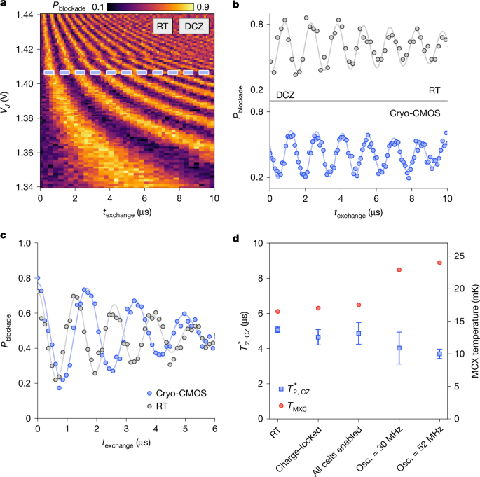
Finally, we turn to evaluate two-qubit logic gates, which provide the most stringent test for crosstalk or electrical noise stemming from proximal milli-kelvin CMOS control. Here, the target qubit is rotated about the z-axis depending on the state of the control qubit, with the gate-tunable exchange interaction modulating the coupling between the two electrons1,24. As a baseline, we first perform a decoupled controlled phase gate (DCZ) using all room temperature instrumentation. The DCZ gate incorporates a spin-echo sequence with coherent rotation about the z-axis of angle ϕ = J(ϵ)texchangeħ, enabled by turning on exchange for a controlled time with J-gate pulse of duration texchange (Extended Data Fig. 2d). The resulting readout probability with J-gate pulse width is shown in Fig. 4a. The DCZ gate is sensitive to high-frequency electrical noise arising either directly from exchange-gate voltage fluctuations or indirectly from noise in the (gradient) magnetic field or variation in g-factors from gate-induced movement in the position of the electron wavefunction.
a, DCZ oscillations as a function of exchange time texchange and VJ, performed using room-temperature (RT) control. b, Room-temperature- and cryo-CMOS-enabled DCZ oscillations at a set VJ, indicated in a. Set level is determined by Vhold, which can be tuned for stronger qubit interaction. c, Comparison of visibility between room-temperature and cryo-CMOS control using identical pulsing methods on all gates. Increased state preparation and measurement error is present because of two-level-only approach to pulsing VJ. d, CZ coherence times of our two-qubit control conditions under various cryo-CMOS parameters. J pulses are generated by cryo-CMOS unless otherwise indicated. Each data point is the average of 100 shots, with 4 repeats for a total of 400 single shots. Error bars represent the 95% confidence level. Osc., oscillator.
Comparing cryo-CMOS control with our room-temperature baseline, we observe that the coherent exchange oscillations show similar behaviour (Fig. 4b). These results immediately confirm the utility of proximal milli-kelvin CMOS for controlling two-qubit logic gates. Close inspection perhaps suggests a suppression in visibility for the CMOS data, which probably stems from the limited two-state resolution of the voltage pulses used to tune the readout and preparation state, which for this qubit device require significantly different tunnel rates than those used in two-qubit control. Although it is not uncommon to find tunnel rates that are very similar for qubit control as state preparation and measurement (SPAM), in the present device, the differing tunnel rates precluded more quantitative measures of SPAM error and two-qubit fidelity using cryo-CMOS35. Future improvements in qubit tunability and fidelity will also enhance sensitivity to new noise sources, including further assessment of the control platform.
As a noise diagnostic tool, it is also worth noting that the DCZ gate is limited because the spin-echo sequence decouples the spin dynamics from low-frequency noise. Removing the echo pulses then opens the bandwidth to now include all of the low-frequency components down to quasi-d.c., offering a better measure of the total aggregate noise inherent in the system. A comparison of room-temperature control and cryo-CMOS is made in the data shown in Fig. 4c, now without spin-echo. These datasets constitute a measure of the ensemble average coherence time associated with the exchange gate, \(T_2,\rmCZ^* \). Finally, using this parameter as a wideband measure of noise, Fig. 4d compares \(T_2,\rmCZ^* \) for room-temperature control, cryo-CMOS with a single charge-locked cell, all 32 cells locked (mirroring J-gate pulses), and as a function of CMOS oscillator frequency. A slight reduction in \(T_2,\rmCZ^* \) (around 20%) is observed at the highest clock frequencies, which, given the slight corresponding increase in refrigerator temperature, can be explained as arising from parasitic heating (for more detailed two-qubit performance data see Extended Data Fig. 5). We note that no additional (electrical) noise is observed beyond the thermal noise contribution associated with the small increase in temperature from CMOS power dissipation (for further discussion, see Extended Data Fig. 4).


