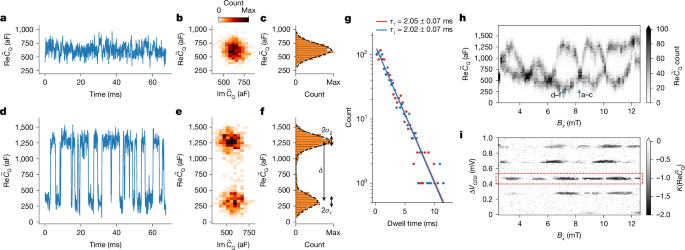
To measure a time record of the fermion parity, we tune up the TQDI and perform a sequence of nearly 1.5 × 10⁴ consecutive measurements of the resonator response, each with an integration time of 4.5 μs, thereby recording a time trace of total length 67 ms. To improve visibility and compare with theoretical predictions, we downsample the time trace by averaging over a 90-μs window. By comparing the measured resonator response with a reference trace (taken with dot 2 in a Coulomb valley), we convert it to a \(\widetildeC_\rmQ\) record, which includes a field-dependent shift of CQ that cancels out of ΔCQ (see equation (28) in the Supplementary Information).
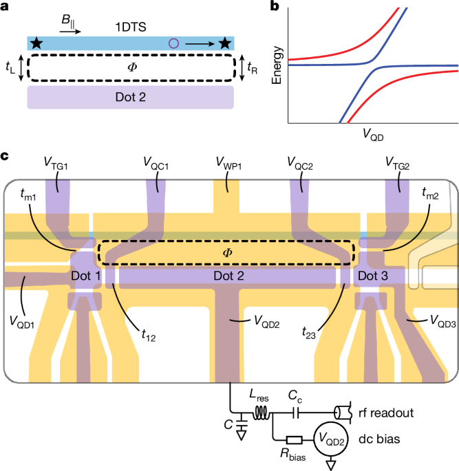
We sweep VQD2 to find charge transitions in dot 2 and, because the normal to the plane of the device is only slightly offset (<1°) from the x axis of the magnet, we sweep the x component of the magnetic field Bx in steps of 0.14 mT to study the dependence on Φ. Our Bx sweep range is offset from 0 so that B⊥ (which contains a contribution from Bz) is swept symmetrically around 0. We use the topological gap protocol (TGP)14 to select an in-plane field B∥ and a wire plunger gate voltage VWP1 range (indicated, respectively, in Fig. 1a,c) for our measurements, as discussed in Section 4 of the Supplementary Information. The readout system parameters that we achieve are not strongly dependent on these values. For measurement A1 of device A, the relevant regime is B∥ ≈ 1.8 T and VWP1 ≈ −1.832 V.
For appropriately tuned quantum dot plungers, in particular for VQD2 close to resonance, the measured \(\widetildeC_\rmQ\) record exhibits switches between two capacitance values that differ by a ΔCQ(Bx) that oscillates as a function of Bx. At some Bx, there are no visible switches, as in Fig. 3a, so ΔCQ(Bx) vanishes. At generic Bx, there is a clear random telegraph signal (RTS), which is shown in Fig. 3d for the Bx that corresponds to maximal ΔCQ(Bx). From a histogram of all \(\widetildeC_\rmQ\) observed within this time trace, we extract an achieved SNR of 5.01 in 90 μs (Fig. 3e,f) or, equivalently, an SNR of 1 in 3.6 μs (see Section 3.3 of the Supplementary Information). As demonstrated in Fig. 3g, the intervals between switches follow an exponential distribution with a characteristic time τRTS ≈ 2 ms. By plotting histograms of the \(\widetildeC_\rmQ\) time traces as a function of Bx, as shown in Fig. 3h, we observe a Bx-dependent bimodal distribution of \(\widetildeC_\rmQ\) values with peaks separated by ΔCQ(Bx). The oscillation period of ΔCQ(Bx) is 1.9 ± 0.1 mT, which is consistent with the expected flux of h/2e through the interference loop in this device geometry. We interpret the RTS in CQ as originating from switches of the fermion parity in the wire; see Section 7.3 of the Supplementary Information for details.
Measurements in device A (measurement A1) in the (B∥, VWP1) parameter regime identified through the tune-up procedure discussed in the main text and Section 4 of the Supplementary Information; specifically, VWP1 = −1.8314 V and B∥ = 1.8 T. The raw rf signal has been converted to complex \(\widetildeC_\rmQ\) by the method described in Section 3.1 of the Supplementary Information. a,d, Time traces at Bx values corresponding to minimal (panel a) and maximal (panel d) values of ΔCQ for a fixed choice of VQD2 close to charge degeneracy. b,e, Histograms of complex \(\widetildeC_\rmQ\) for the time trace shown in panels a and d. c,f, Histograms of the real part \(\rmRe\widetildeC_\rmQ\) with Gaussian fits for an extraction of the SNR = δ/(σ1 + σ2) = 5.01, the details of which are given in Section 3.3 of the Supplementary Information. g, Histogram of dwell times aggregated over all values of Bx, in which the signal shows bimodality. Fitting to an exponential shows that the up and down dwell times agree to within the standard error on the fits: 2.05 ± 0.07 ms and 2.02 ± 0.07 ms, respectively. h, Histogram of \(\widetildeC_\rmQ\) values as a function of Bx, showing clear bimodality that is flux-dependent with period h/2e. The vertical arrows indicate the Bx values at which the time traces in panels a and d were taken. i, Kurtosis in the measured quantum capacitance, \(K(\textRe\widetildeC_\rmQ)\), of dot 2 as a function of Bx (which controls Φ) and ΔVQD2, the change in dot plunger gate voltage from the starting point of the scan (which controls the dot 2 detuning). The dashed red rectangle indicates the ΔVQD2 value at which the data in the other panels were taken.
The visibility and phase of the oscillations vary between successive charge transitions in dot 2. We illustrate this by showing the kurtosis K(CQ) (which detects bimodality; see Section 3.2 of the Supplementary Information) of the \(\widetildeC_\rmQ\) time traces for several different charge transitions in Fig. 3i. A similar difference in the visibility of flux-induced oscillations across different charge transitions was recently observed in a double quantum dot interferometer experiment47. In Section 6 of the Supplementary Information, we discuss oscillations with different periods that are observed at other points in the parameter space of the device.
We support this interpretation by reproducing our results with quantum dynamics simulations that incorporate rf drive power, charge noise and temperature. To build intuition for those simulations, we use an idealized model (see Section 2.2 of the Supplementary Information) subject to the following assumptions (which we will later relax): the wire is in the topological phase and there are no sub-gap states other than the MZMs; the charging energy and level spacing in the dots are much greater than the temperature; dots 1 and 3 are sufficiently detuned that their influence is fully encapsulated in the effective couplings tL and tR to MZMs at the ends of the wire (see Fig. 1a); and the drive frequency and power are both negligible. In this limit, the quantum capacitance as a function of the total fermion parity in the quantum dot–wire system, Z, is given by
$$\beginarraylC_\rmQ(Z\,,\phi )\,=\,\frac t_\rmC(Z\,,\phi ) ^2{[(E_\rmD+2ZE_\rmM)^2+4^3/2}\\ \,\,\,\,\,\times \,\tanh \left(\frac{\sqrt(E_\rmD+2ZE_\rmM)^2+4}2k_\rmBT\right),\endarray$$
(1)
in which ED is the detuning from the charge-degeneracy point, α is the lever arm of the plunger gate to the dot, EM is the MZM energy splitting and T is the temperature. The net effective tunnelling that results from the interference between different trajectories from the dot to the MZMs and back, tC(Z, ϕ), is
$$| t_\rmC(Z\,,\phi ) ^2=| t_\rmL ^2+| t_\rmR ^2+2Z| t_\rmL| | t_\rmR| \sin \phi .$$
(2)
Here ϕ is the phase difference between tL and tR, which is controlled by the magnetic flux Φ through the interference loop created by the dot, the wire and the tunnelling paths between them according to ϕ = 2πΦ/Φ0 + ϕ0, in which Φ0 = h/e and ϕ0 is a flux-independent offset. To capture the extent to which CQ can be used to discriminate between Z = ±1, it is convenient to introduce
$$\Delta C_\rmQ(\phi )=| C_\rmQ(Z=1,\phi )-C_\rmQ(Z=-1,\phi )| .$$
(3)
The interferometer must be well balanced tL ≈ tR for ΔCQ to be large according to equation (1). When EM = 0, ΔCQ exhibits maxima along the ED = 0 line, with flux periodicity h/2e.
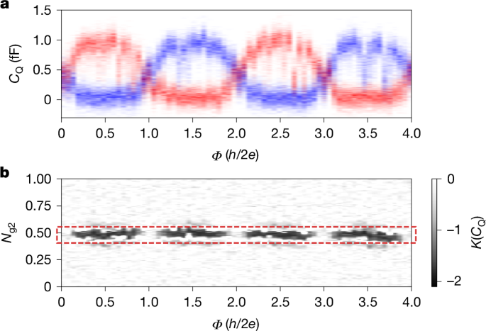
For detailed comparison with experiments, we use the methods discussed in Sections 2.4 and 2.5 of the Supplementary Information to simulate a more complete model of the device and readout chain that includes the full triple-dot system, incoherent coupling to the environment (using parameters inferred from separate measurements; see Sections 9 and 10 of the Supplementary Information) and measurement backaction. Crucially, this approach allows us to incorporate different noise sources in a systematic and quantitative way without any free parameters. The simulated dynamical CQ, defined in Section 2.3 of the Supplementary Information, is shown in Fig. 4. The CQ histograms in Fig. 4a reveal two h/e-periodic branches (one shown in red and the other in blue), associated with the two parities of the coupled system. If the fermion parity Z were perfectly conserved, then the device would remain in one of the two parity eigenstates and the Φ dependence would follow either the blue or the red trace in Fig. 4a. However, Z should fluctuate on a timescale given by the quasiparticle poisoning time τqpp. Hence, in traces over times longer than τqpp, a bimodal distribution of CQ values is expected, that is, both the blue and red traces in Fig. 4a. Consequently, the kurtosis K(CQ) exhibits minima at which ΔCQ is peaked, as shown in Fig. 4b, and time traces taken at these points will exhibit a telegraph signal composed of switches between the values CQ(1, ϕ) and CQ(−1, ϕ). Comparing Fig. 4 with Fig. 3h,i, we find good overall agreement of both the histograms and the kurtosis. We find a maximum ΔCQ(Φ) ≈ 1 fF, which is consistent with our measurements in Fig. 3. This agreement extends to other parameter regimes, such as when the interferometer is poorly balanced or the splitting EM is sizeable, as discussed in Section 6 of the Supplementary Information.
Simulated dynamical CQ as a function of magnetic flux and dot 2 gate offset charge Ng2, including the effects of charge and readout noise, as well as non-zero temperature, drive power and frequency, per the discussion in the text. a, Histogram of the two parity sectors for fixed Ng2 = 0.49. Here we used tm1 = tm2 = 6 μeV, t12 = t23 = 8 μeV, EC1 = 140 μeV, EC2 = 45 μeV, EC3 = 100 μeV, Ng1 = Ng3 = 0.3, T = 50 mK and EM = 0. b, Kurtosis of CQ(t) as a function of Ng2 and flux through the loop. The middle of the dashed red rectangle indicates the Ng2 value used for the linecut in panel a.
A second measurement of device A and a measurement of a second device (device B) give results in qualitative agreement with those of measurement A1, demonstrating the reproducibility of the observed phenomena (Section 5 of the Supplementary Information). We have tested our interpretation by: (1) disconnecting the dots from the wire; (2) measuring at fields of 0.8 T below the region identified by TGP; (3) intentionally injecting quasiparticles into the superconductor and observing the effect on τRTS; and (4) comparing the quasiparticle density measured in a separate test structure with that inferred according to the hypothesis that τqpp = τRTS ≈ 2 ms (Section 7 of the Supplementary Information).
By extending the model introduced above, we have analysed the quasi-MZM scenario discussed in previous works37,38,39,48. We introduce an extra pair of ‘hidden’ Majorana modes that are weakly coupled to each other and to the visible MZMs, which themselves are coupled to quantum dots 1 and 3. Together, the hidden and visible MZMs form a trivial low-energy state at each end of the wire. This scenario can occur in the trivial phase, in which it requires some fine-tuning to make the couplings small. In Section 2.7 of the Supplementary Information, we show that the hidden Majorana modes suppress ΔCQ owing to fast fermion tunnelling between them and the visible MZMs. This effect completely washes out the flux-dependent bimodality unless the coupling between the ‘hidden’ Majorana modes and the visible MZMs is less than 1 neV or the hidden Majorana modes are effectively gapped out, as shown in Supplementary Fig. 4.


