


Credit: Olivier Morin/AFP via Getty
George E. Smith’s collaboration with Willard Boyle at Bell Labs in Murray Hill, New Jersey, led to the invention of the charge coupled device (CCD) in October 1969. Over an hour’s brainstorming session, in which they set out to design a memory device, the two engineers came up with an idea about how to move electrons between capacitors in a semiconductor. Owing to the dynamic and research-focused nature of Bell Labs, the idea was implemented in silicon just a week after it was conceived (W. S. Boyle and G. E. Smith Bell Syst. Tech. J. 49, 587–593; 1970), and proved ideally suited to capturing images. Boyle and Smith shared half of the 2009 Nobel Prize in Physics “for the invention of an imaging semiconductor circuit — the CCD sensor”.
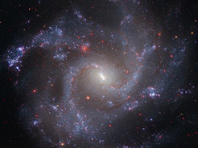
The invention was subsequently part of the Hubble Space Telescope (HST) and other space missions, transforming their ability to photograph astronomical objects, and was incorporated into many other applications including television cameras, medical radiography and digital consumer products. CCDs detect light using the photoelectric effect: the emission of electrons when light hits a material. They are sensitive to wavelengths between 300 and 1,000 nanometres. Absorbed photons liberate electrons, so they drift under the influence of whatever electric fields are present.
The challenge for CCD designers is to manipulate such fields to ensure that these photoelectrons are collected efficiently and stored without loss during exposure. Once the shutter closes and the read-out begins, this charge then needs to be converted to a voltage signal and digitized with as little extra noise as possible. The genius of the CCD design is that the same structures that the device uses to collect light also transfer the photo-generated charge to a measurement amplifier at the edge of the detector once the exposure has finished.
Will AI jeopardize science photography? There’s still time to create an ethical code of conduct
Smith was born in White Plains, New York, in 1930. After four years in the US Navy, he studied physics at the University of Pennsylvania in Philadelphia before gaining his PhD at the University of Chicago, Illinois, in 1959. He then moved to Bell Labs, and worked under Boyle, studying the electronic properties of semi-metals and low-temperature electronic technologies, before Boyle made him head of the new device concepts group.
At the time they invented CCDs, exploiting the earlier Bell Labs invention of metal–oxide–semiconductor capacitors, Smith was working on a videophone based on a silicon-diode-array camera tube. It was never developed because of the difficulties of manufacturing chips with one million perfect diodes, but his exploration of digital imaging helped the Bell team to realize the potential of CCDs for that purpose.
The expanding Universe — do ongoing tensions leave room for new physics?