Ahmadi, M., Wu, T. & Hu, B. A review on organic–inorganic halide perovskite photodetectors: device engineering and fundamental physics. Adv. Mater. 29, 1605242 (2017).
Chen, J. et al. Highly efficient and stable perovskite solar cells enabled by low-dimensional perovskitoids. Sci. Adv. 8, eabk2722 (2022).
Shi, E. et al. Two-dimensional halide perovskite nanomaterials and heterostructures. Chem. Soc. Rev. 47, 6046–6072 (2018).
Song, K. et al. Atomic-resolution imaging of halide perovskites using electron microscopy. Adv. Energy Mater. 10, 1904006 (2020).
Zhang, D. et al. Atomic-resolution transmission electron microscopy of electron beam–sensitive crystalline materials. Science 359, 675–679 (2018).
Dong, Y. et al. The role of surface termination in halide perovskites for efficient photocatalytic synthesis. Angew. Chem. 132, 13031–13037 (2020).
Mariotti, S. et al. Interface engineering for high-performance, triple-halide perovskite–silicon tandem solar cells. Science 381, 63–69 (2023).
Al-Ashouri, A. et al. Monolithic perovskite/silicon tandem solar cell with > 29% efficiency by enhanced hole extraction. Science 370, 1300–1309 (2020).
Jiang, Q. et al. Surface passivation of perovskite film for efficient solar cells. Nat. Photon. 13, 460–466 (2019).
Zhang, S. et al. Minimizing buried interfacial defects for efficient inverted perovskite solar cells. Science 380, 404–409 (2023).
Dou, L. et al. Atomically thin two-dimensional organic-inorganic hybrid perovskites. Science 349, 1518–1521 (2015).
Lee, J.-W., Tan, S., Seok, S. I., Yang, Y. & Park, N.-G. Rethinking the a cation in halide perovskites. Science 375, eabj1186 (2022).
Zhao, Y. et al. Suppressing ion migration in metal halide perovskite via interstitial doping with a trace amount of multivalent cations. Nat. Mater. 21, 1396–1402 (2022).
Li, C. et al. Rational design of Lewis base molecules for stable and efficient inverted perovskite solar cells. Science 379, 690–694 (2023).
Wang, R. et al. Constructive molecular configurations for surface-defect passivation of perovskite photovoltaics. Science 366, 1509–1513 (2019).
Yang, S. et al. Stabilizing halide perovskite surfaces for solar cell operation with wide-bandgap lead oxysalts. Science 365, 473–478 (2019).
Ball, J. M. & Petrozza, A. Defects in perovskite-halides and their effects in solar cells. Nat. Energy 1, 16149 (2016).
Rothmann, M. U. et al. Atomic-scale microstructure of metal halide perovskite. Science 370, eabb5940 (2020).
Zhang, S. et al. Deterministic synthesis of a two-dimensional MAPbI3 nanosheet and twisted structure with moiré superlattice. J. Am. Chem. Soc. 146, 27861–27870 (2024).
Yang, H. et al. Simultaneous atomic-resolution electron ptychography and z-contrast imaging of light and heavy elements in complex nanostructures. Nat. Commun. 7, 12532 (2016).
Pennycook, T. J., Martinez, G. T., Nellist, P. D. & Meyer, J. C. High dose efficiency atomic resolution imaging via electron ptychography. Ultramicroscopy 196, 131–135 (2019).
Li, G., Zhang, H. & Han, Y. 4D-STEM ptychography for electron-beam-sensitive materials. ACS Cent. Sci. 8, 1579–1588 (2022).
Wang, Z. et al. Ptychographic observation of lithium atoms in the irradiation-sensitive garnet-type solid electrolyte at sub-angstrom resolution. J. Am. Chem. Soc. 147, 18025–18032 (2025).
Zhang, H. et al. Three-dimensional inhomogeneity of zeolite structure and composition revealed by electron ptychography. Science 380, 633–638 (2023).
Chen, Z. et al. Mixed-state electron ptychography enables sub-angstrom resolution imaging with picometer precision at low dose. Nat. Commun. 11, 2994 (2020).
Sha, H. et al. Ptychographic measurements of varying size and shape along zeolite channels. Sci. Adv. 9, eadf1151 (2023).
Song, J. et al. Atomic resolution defocused electron ptychography at low dose with a fast, direct electron detector. Sci. Rep. 9, 3919 (2019).
Jannis, D., Velazco, A., Béché, A. & Verbeeck, J. Reducing electron beam damage through alternative STEM scanning strategies, part II: attempt towards an empirical model describing the damage process. Ultramicroscopy 240, 113568 (2022).
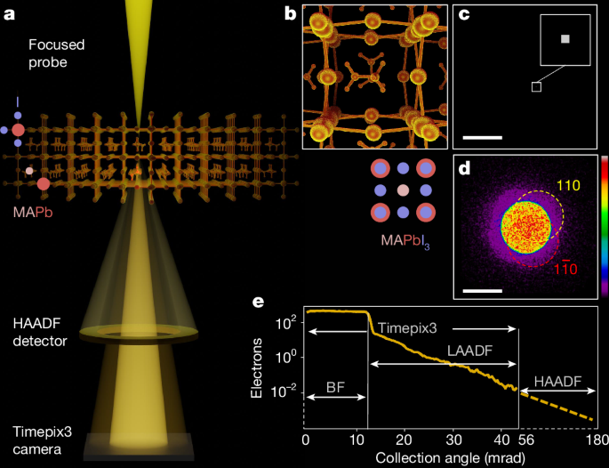
Jannis, D. et al. Event driven 4D STEM acquisition with a Timepix3 detector: microsecond dwell time and faster scans for high precision and low dose applications. Ultramicroscopy 233, 113423 (2022).
Maiden, A. M. & Rodenburg, J. M. An improved ptychographical phase retrieval algorithm for diffractive imaging. Ultramicroscopy 109, 1256–1262 (2009).
Pennycook, T. J. et al. Efficient phase contrast imaging in STEM using a pixelated detector. part 1: experimental demonstration at atomic resolution. Ultramicroscopy 151, 160–167 (2015).
Maiden, A. M., Mei, W. & Li, P. WASP: weighted average of sequential projections for ptychographic phase retrieval. Opt. Express 32, 21327–21344 (2024).
Gao, C. et al. Overcoming contrast reversals in focused probe ptychography of thick materials: an optimal pipeline for efficiently determining local atomic structure in materials science. Appl. Phys. Lett. 121, 081906 (2022).
Clark, L. et al. The effect of dynamical scattering on single-plane phase retrieval in electron ptychography. Microsc. Microanal. 29, 384–394 (2023).
Hofer, C., Gao, C., Chennit, T., Yuan, B. & Pennycook, T. J. Phase offset method of ptychographic contrast reversal correction. Ultramicroscopy 258, 113922 (2024).
Zhang, S. et al. Moiré superlattices in twisted two-dimensional halide perovskites. Nat. Mater. 23, 1222–1229 (2024).
Quarti, C., De Angelis, F. & Beljonne, D. Influence of surface termination on the energy level alignment at the CH3NH3PbI3 perovskite/C60 interface. Chem. Mater. 29, 958–968 (2017).
Mirzehmet, A. et al. Surface termination of solution-processed CH3NH3PbI3 perovskite film examined using electron spectroscopies. Adv. Mater. 33, 2004981 (2021).
Kim, T. et al. Mapping the pathways of photo-induced ion migration in organic-inorganic hybrid halide perovskites. Nat. Commun. 14, 1846 (2023).
Jeong, J. et al. Pseudo-halide anion engineering for α-FAPbI3 perovskite solar cells. Nature 592, 381–385 (2021).
Yuan, B. et al. Atomically resolved edges and defects in lead halide perovskites. Zenodo https://doi.org/10.5281/zenodo.11482207 (2025).


