As silicon (Si) field-effect transistors (FETs) approach the fundamental limits in scaling, new generations of semiconducting channels are required to reduce the short-channel effects1,2. Two-dimensional (2D) materials such as molybdenum disulfide (MoS2), which is atomically thin and has high carrier mobility, thus have huge potential in future transistors4,8,9,10. Although 2D materials have better physical and electrical properties than Si, suitable high-quality dielectric materials are not available. Therefore, FET devices based on 2D materials cannot fulfil the full potential predicted theoretically5,6. Amorphous oxide dielectrics that work well in Si technology, for example, SiO2, Al2O3 and HfO2, cannot provide a uniform and well-defined interface with 2D materials because of the disruption of long-range orders11,12,13. Considering the amorphous nature and ill-defined interfaces, there are difficulties in eliminating charge scattering and traps, thus resulting in (1) high gate leakage current (Jâ>â1.5âÃâ10â2âAâcmâ2), (2) high interface state density (Ditâ>â1010âcmâ2âeVâ1) and (3) low dielectric strength (Ebdâ<â10âMVâcmâ1), which cannot meet the requirements stipulated by the International Roadmap for Devices and Systems (IRDS)3,5,7. Moreover, owing to the inert dangling-bond-free surface of 2D materials, depositing an atomically thin oxide without damaging the adjacent layer remains challenging6.
Compared with amorphous oxides, crystalline dielectric materials such as hexagonal boron nitride (hBN)14, calcium fluoride (CaF2) (ref.â11) and perovskite strontium titanium oxide (SrTiO3) (ref.â13) have atomically flat surfaces that bond well for smoother dielectric/2D material interfaces. In theory, these materials can overcome the problems of interface quality and defect bands. However, there are some disadvantages of crystalline dielectrics. For example, because of the relatively narrow bandgap and low permittivity, hBN with an ultrathin physical thickness exhibits extremely high leakage currents (Jâ>â103âAâcmâ2) (ref.â15). The use of CaF2 and SrTiO3 is limited to back-gate FETs11,13, although large-scale integrated circuits require top-gate 2D FETs. The unique advantage that Bi2SeO5 offers is inherently tied to its semiconducting counterpart, which means it may not provide the same benefits when paired with other 2D materials16. Other crystalline dielectrics, such as mica, have difficulty in precisely controlling the area and thickness of insulators generated by exfoliation or chemical growth methods17. Furthermore, it is challenging to attain an interface state density of 1010âcmâ2âeVâ1 from devices comprising crystalline dielectrics. Moreover, wafer-scale synthesis of high-quality crystalline dielectrics is quite challenging11,13,16,17. As there is still no clear strategy on how to scale dielectrics down to be atomically thin as required by commercial FETs5,6, it may be necessary to identify radically different approaches for 2D devices.
Atomically thin metal oxides have attracted attention recently because of their unique electronic, optical and magnetic properties that are rarely found in their bulk counterparts18,19. By adopting simple oxidation, a stable, stoichiometric and atomically thin oxide layer can be formed on the metal surface for 2D devices18,19. So far, oxides made of transition metals such as HfO2, TiO2, Fe2O3 and Ni2O3; post-transition metals such as Al2O3; and rare earth metals, including Gd2O3, have been proposed18,19. These atomically thin metal oxides have adequate dielectric properties and atomically flat surfaces, making them suitable for electrostatic modulation of the channels of 2D materials to overcome the present limitations.
In this study, a single-crystalline Al2O3 (c-Al2O3) is achieved as a high-quality dielectric layer on the 2D MoS2 FET. By combining epitaxial lift-off and intercalative oxidation, an atomically thin c-Al2O3 with a thickness of 1.25ânm is prepared, which is thinner than the conventional oxides used in advanced Si transistors20,21. Owing to the favourable crystalline structure and well-defined interfaces, the gate leakage current (Jâ<â1âÃâ10â6âAâcmâ2), interface state density (Ditâ=â8.4âÃâ109âcmâ2âeVâ1) and dielectric strength (Ebdâ=â17.4âMVâcmâ1) of the atomically thin c-Al2O3 can meet the IRDS requirements for low-power devices3,5. By using the van der Waals (vdW) transfer method, the entire FET stack, including the source, drain, dielectric and gate, can be transferred to the MoS2 channel in a one-step process to produce a 2D FET with excellent contact and dielectric interfaces. The top-gate MoS2 FET shows a steep subthreshold swing (SS) of 61âmVâdecâ1, ultrahigh on/off current ratio of 108 and small hysteresis of 10âmV. Excellent processing reproducibility and uniformity are demonstrated by fabricating a batch of 100 devices.
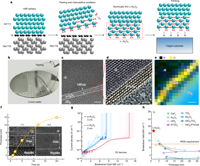
Figure 1a shows a scalable method to synthesize high-quality atomically thin c-Al2O3 layers without complex chemistry or sophisticated equipment. A graphene (Gr)/germanium (Ge) wafer is used as the template, and wafer-scale single-crystalline Al is produced by electron beam evaporation using the vdW epitaxy approach22,23,24. Given that Gr/Ge substrates can be manufactured up to 12 inches in diameter considering the epitaxy of Ge on Si, the industrial-scale production of single-crystalline Al becomes a tangible possibility. The cross-sectional high-resolution transmission electron microscopy (HR-TEM) image and X-ray diffraction results are shown in Extended Data Fig. 1 to confirm the wafer-scale vdW epitaxy of single-crystalline Al(111) on single-crystalline Gr/Ge(110). We proved that a patterned metal with an atomically flat surface can be delaminated from graphene by exploiting the weak vdW force25. In this case, Al can be peeled off readily from graphene and then oxidized mildly at room temperature in the 0.2-ppm oxygen environment. Owing to the atomically flat single-crystalline Al surface and oxygen-deficient environment (0.2âppm O2), homogeneous coverage of chemisorbed oxygen atoms and limited penetration of oxygen can be attained. Consequently, a depolarized c-Al2O3 layer is formed when one oxygen atom chemisorbs on an Al atom, which has been confirmed theoretically and experimentally19. In only a few seconds, an ultrathin c-Al2O3 layer with a thickness of several nanometres is formed by the layer-by-layer mechanism. The cross-sectional HR-TEM image presented in Extended Data Fig. 2 shows the epitaxial relationship between c-Al2O3 (0001) and Al (111). Finally, the atomically thin c-Al2O3 is transferred onto a target substrate such as SiO2, MoS2 or Au to fabricate the device. The fabrication details are presented in the Methods and Extended Data Fig. 3. To prevent Al from oxidizing in H2O, the entire process is water-free. Moreover, benefiting from the water-free transfer process, the graphene surface is not damaged thereby allowing repeated use of the Gr/Ge wafer (Extended Data Fig. 4).
a, Fabrication of atomically thin c-Al2O3 through epitaxial lift-off and intercalative oxidation of a single-crystalline Al film. b, Optical image of the lift-off of Al/c-Al2O3 from a 4-inch Gr/Ge wafer. c, A cross-sectional HR-TEM image of Al/c-Al2O3 on a target SiO2 substrate. d, Magnified atomic-resolution image from the red box in c. e, EEL mapping of Al/c-Al2O3/SiO2. f, The relationship between exposure time in an oxygen-deficient environment (0.2âppm O2) and the thickness of c-Al2O3. Insets, the cross-sectional HR-TEM image of c-Al2O3 with a thickness of 2ânm and 6ânm obtained by 1âh oxidation and 5âh oxidation, respectively. g, The breakdown field of c-Al2O3 and a-Al2O3. h, The breakdown field compared with film thickness for various dielectrics. Scale bars, 2ânm (c); 1ânm (d,e).
Figure 1b shows that the lift-off Al/c-Al2O3 has close to 100% yield as evidenced by delamination of the 4-inch patterned Al film from the Gr/Ge substrate using polyvinyl alcohol; Supplementary Video 1 shows the entire peeling process. The lifted-off c-Al2O3 films are transferred onto the SiO2 substrate, and the cross-sectional HR-TEM image is shown in Fig. 1c. The thickness of the c-Al2O3 layer on the Al surface is about 1.25ânm. The magnified atomic-resolution image of the red box in Fig. 1c is shown in Fig. 1d disclosing the sandwiched structure of Al/c-Al2O3/SiO2. Electron energy loss spectroscopy (EEL) mapping shows the elemental distributions (Fig. 1e), and the distributions of Al and O are in accordance with the sandwiched structure.
Moreover, the thickness of c-Al2O3 can be manipulated by exposing the vdW epitaxial Al layer to an oxygen-deficient environment for various durations. As shown in Fig. 1f, as the oxidation time is increased from 1âh to 12âh, the oxidation rate decreases from 2ânmâhâ1 to 0.8ânmâhâ1. This is because the oxidation process is controlled by the interface reaction at first and then by oxygen diffusion16. Figure 1f (insets) shows the cross-sectional HR-TEM image of c-Al2O3 with thicknesses of 2ânm (oxidation for 1âh) and 6ânm (oxidation for 5âh), and more HR-TEM images are shown in Extended Data Fig. 5. The results confirm that it is possible to prepare c-Al2O3 layers with different thicknesses by controlling the oxidation time. Moreover, the thickness mapping of the 4-inch c-Al2O3/Al wafer is shown in Supplementary Fig. 1 and Supplementary Table 1, which indicates the exceptionally uniform coefficient of variation of ±6%.
Figure 1g shows the breakdown field (Ebd) compared with the current density trend. c-Al2O3 remains completely insulating for the operating fields well above the IRDS requirement of 10âMVâcmâ1. The average Ebd determined from 20âmetalâinsulatorâmetal (MIM) devices with the c-Al2O3 insulator is 16âMVâcmâ1 and the maximum is 17.4âMVâcmâ1. In comparison, the amorphous Al2O3 (a-Al2O3) layer with a thickness of 5ânm fabricated by lifting off the Al film in an ambient environment exhibits a small average Ebd of about 8âMVâcmâ1 similar to the previous studies26,27. The enhancement of Ebd may arise from the energy gap increment or the defect density reduction in crystalline insulators5,28. The Ebd versus film thickness for different metal oxides is compared in Fig. 1h, and the details are provided in Supplementary Table 2. Owing to the crystalline structure and large bandgap (8.8âeV) (refs.â26,28), defect-assisted tunnelling in c-Al2O3 is suppressed. As a result, the atomically thin c-Al2O3 exhibits one of the highest Ebd (17.4âMVâcmâ1) compared with amorphous oxides (TiO2 (ref.â29), Al2O3 (ref.â30) and HfO2 (refs.â31,32,33) as well as single-crystalline oxides (CaF2 (ref.â34), SrTiO3 (ref.â13) and Sb2O3 (ref.â12)). It is important to note that Ebd of c-Al2O3 exceeds the IRDS requirement for low-power devices (Ebdâ>â10âMVâcmâ1) (refs.â3,5).
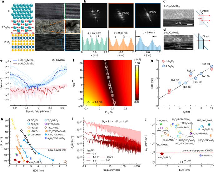
The gate leakage currents (J) and interface state densities (Dit) are important properties of low-power devices, and J and Dit should be less than 1.5âÃâ10â2âAâcmâ2 and 1010âcmâ2âeVâ1, respectively, to meet the IRDS requirements for low-power devices3,5,32. However, it is challenging to meet these stringent requirements for 2D devices because the amorphous oxide cannot provide a well-defined interface5,32, whereas crystalline dielectric materials are easy to form an abrupt interface with 2D channel, but some of them, for example, Sb2O3 (ref.â12), SrTiO3 (ref.â13), h-BN (ref.â15), have a relatively small bandgap. It is possible to address these problems by using single-crystalline c-Al2O3 because it has an adequate bandgap of 8.8âeV compared with other high-κ oxides26. To determine the Al/c-Al2O3 gate properties, the structure is transferred onto the multilayer MoS2 to form the Al/c-Al2O3/MoS2 heterostructure (Fig. 2a). The cross-sectional HR-TEM image of the heterostructure shows a stack consisting of single-crystalline Al, c-Al2O3 and MoS2 layers, from top to bottom, respectively. An atomically sharp interface is observed between c-Al2O3 and MoS2. The magnified images of the dashed green, orange and blue boxes in Fig. 2a (right) indicate single-crystalline Al, c-Al2O3 and MoS2, respectively. Figure 2b shows the selected area electron diffraction patterns of the dashed green, orange and blue boxes in Fig. 2a confirming the crystallinity of each stacked region. The line profiles (Fig. 2b, bottom) along the dashed green, orange and blue lines in Fig. 2a show periodic variability in the interatomic distance. The distances for Al, c-Al2O3 and MoS2 are derived to be 0.21ânm, 0.37ânm and 0.6ânm, respectively.
a, Schematic (left), cross-sectional HR-TEM (middle) and magnified atomic-resolution (right) images of an Al/c-Al2O3/MoS2 heterostructure. b, Selected area electron diffraction patterns (top) obtained from the dashed green, orange and blue boxes in a. Line intensity profiles (bottom) along the dashed green, orange and blue lines in a. c, HR-TEM image of a-Al2O3/MoS2 (left) and the important tunnelling contributions (right). d, HR-TEM image of c-Al2O3/MoS2 (left) and the important tunnelling contributions (right). e, Experimental gate leakage currents for 2D FETs with c-Al2O3 and a-Al2O3. f, The relationship between current and gate voltage. VTG, top-gate voltage; VBG, back-gate voltage. g, The relationship between EOT and dielectric thickness. h, Experimental gate leakage currents compared with EOT measured at standard operating gate voltages of 1âV. i, Noise power spectra as a function of frequency. j, Comparison of Dit values measured for Si devices and different 2D technologies. Scale bars, 5ânm (a, bottom row, middle); 2ânm (a, bottom row, right); 2ânm (c,d). TAT, trap-assisted tunnelling.
Two different types of Al2O3 dielectric materials, amorphous and crystalline, are transferred onto the MoS2 channel by the same integration method. The HR-TEM images of a-Al2O3/MoS2 are shown in Fig. 2c (left) and those of c-Al2O3/MoS2 are shown in Fig. 2d (left). The important tunnelling contributions of the a-Al2O3/MoS2 junctions are shown in Fig. 2c (right) and those of the c-Al2O3/MoS2 junctions are shown in Fig. 2d (right). Apart from direct tunnelling through a-Al2O3, trap-assisted tunnelling, which is observed in insulators containing a substantial number of defects, plays an important part. Conversely, these tunnelling currents are suppressed because c-Al2O3 has a wider bandgap and a smaller defect density. Figure 2e shows the experimental J values of c-Al2O3/MoS2 and a-Al2O3/MoS2, and c-Al2O3/MoS2 shows a J value that is about two orders of magnitude lower than that of a-Al2O3/MoS2.
A double-gate device with SiO2/Si as the global back gate and Al/c-Al2O3 as the top-gate stack is fabricated to measure the equivalent oxide thickness (EOT) accurately. The top-gate capacitance (CTG) is extracted experimentally as shown in Extended Data Fig. 6. The EOT is calculated to be 1.4ânm (Fig. 2f) using the equation EOTâ=â3.45/CTG (ref.â32). Furthermore, six devices with different EOTs are fabricated as shown in Extended Data Fig. 6. Figure 2g compares the EOT values for different dielectric thicknesses (td). The comparison of the dielectric constant with td is shown in Supplementary Fig. 2. As expected, EOT increases linearly with td for both a-Al2O3 (refs.â35,36,37,38,39) and c-Al2O3, which is consistent with the equation EOTâ=â3.9td/εd, where εd is the dielectric constant of Al2O3 (refs.â30,40). Specifically, c-Al2O3 shows the smallest EOT compared with other 2D devices based on Al2O3 reported so far and also demonstrates the potential for scaling down 2D FETs.
The J values of other typical amorphous oxide dielectrics20,21,32,41,42,43,44, c-Al2O3 dielectrics and crystalline dielectrics11,13,15 with varying EOTs are provided in Fig. 2h. Except for hBN, the crystalline dielectric materials with a well-defined interface have a smaller J than conventional amorphous oxides. As a result of the small bandgap and low permittivity, 2D hBN exhibits extremely high J values15. The c-Al2O3/MoS2 device shows a J value of 10â6âAâcmâ2, which is four orders of magnitude lower than the low-power requirement (10â2âAâcmâ2) by IRDS3,32. Moreover, the J values (EOTâ=â0.77ânm; Supplementary Fig. 3) are steady even when the temperature increases to about 403âK (Supplementary Fig. 4), indicating that the trap-assisted tunnelling phenomenon in amorphous dielectric materials is hardly seen in c-Al2O3. Another comparison between c-Al2O3/MoS2 and the mature Si-CMOS technology shows that J is five orders of magnitude lower than that of Al2O3/Si (ref.â20), suggesting great scaling-down potential for the c-Al2O3/MoS2 FETs.
The interface state density (Dit) is determined by the 1/f noise method30 as shown in Fig. 2i. Because of the well-defined interface between c-Al2O3 and MoS2, a reduced Dit of 8.4âÃâ109âcmâ2âeVâ1 is achieved, similar to the value measured by the capacitanceâvoltage method (Supplementary Fig. 5). The calculation details are described in the Methods. The comparison of the Dit values with those in the literature is presented in Fig. 2j, and the details are shown in Supplementary Table 3. Most of the Dit values of exfoliated MoS2 channels are high ranging from 5âÃâ1011âcmâ2âeVâ1 to 1013âcmâ2âeVâ1 for both conventional amorphous oxide dielectrics31,32,37,43,44,45,46,47,48,49 and crystalline dielectrics11,13,15. In our case, a Dit of 8.4âÃâ109âcmâ2âeVâ1 is achieved from c-Al2O3/MoS2, and it meets the IRDS requirement for low-standby-power CMOS and is comparable to that of Si/SiO2 (Ditâ~â109âcmâ2âeVâ1) (ref.â50).
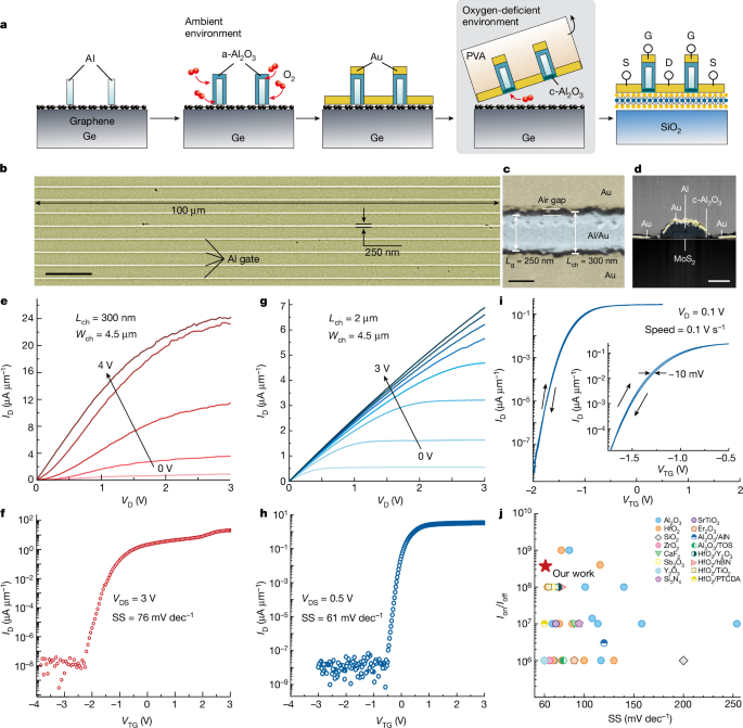
To study the electronic characteristics of the 2D FET based on c-Al2O3, a self-aligned MoS2 FET with 2ânm c-Al2O3 is fabricated by the vdW transfer method. The fabrication process of the self-aligned MoS2 FET is shown in Fig. 3a and Supplementary Fig. 6. Figure 3b shows the scanning electron microscopy (SEM) image of an array of the self-aligned MoS2 FETs. The width and length of the Al gate are 100âμm and 250ânm, respectively. A small air gap between Au and the Al gates, which ensures the complete insulation between the top gate and source or drain and the successful self-alignment process, is shown in Fig. 3c. The channel length is 300ânm (Lchâ=â300ânm). The cross-sectional TEM image of self-aligned MoS2 FET is shown in Fig. 3d. The vdW transfer method enables the fabrication of the complete FET stack by the self-alignment process, including the source, drain, dielectric and gate on the graphene/Ge donor wafer, and then it is transferred onto the channel materials in a one-step lamination process to produce the 2D FET with a good contact and dielectric interfaces48.
a, The fabrication process of a self-aligned c-Al2O3/MoS2 FET. b, SEM image of an array of self-aligned MoS2 FETs. c, Magnified SEM image of self-aligned MoS2 FET with a small air gap. d, Cross-sectional TEM image of self-aligned MoS2 FET. e,f, The output (e) and transfer (f) characteristics of a short-channel three-layered MoS2 FET. g,h, The output (g) and transfer (h) characteristics of a long-channel three-layered MoS2 FET. i, The dual-sweep transfer curve. j, Experimental SS values versus Ion/Ioff of MoS2 FETs with various dielectrics. Scale bars, 10âμm (b); 200ânm (c); 100ânm (d).
The output (drain current versus drain voltage, IDâVD) and transfer (drain current versus gate voltage, IDâVTG) characteristics of the MoS2 FET are shown in Fig. 3e,f. The output characteristics demonstrate promising current control and saturation. The drain current of the transfer curves shows a steep increase in the subthreshold region with a subthreshold swing (SS) of about 76âmVâdecâ1 and an on/off current ratio (Ion/Ioff) of 109. The output and transfer characteristics of the long-channel MoS2 FET are shown in Fig. 3g,h. A small SS of 61âmVâdecâ1 (Extended Data Fig. 7) close to the thermal limit of 60âmVâdecâ1 at 300âK is accomplished. A small hysteresis of 10âmV is also observed in the dual-sweep linear transfer curve in Fig. 3i, indicating a low trapping charge density in c-Al2O3. Moreover, a contrast experiment is performed using FETs containing c-Al2O3 and a-Al2O3 (Extended Data Fig. 8). The SS and hysteresis obtained from the device with c-Al2O3 (SSâ=â61âmVâdecâ1 and hysteresis of 40âmV) are notably lower than those of a-Al2O3 (SSâ=â120âmVâdecâ1 and hysteresis of 250âmV). Figure 3j shows the SS versus Ion/Ioff results of MoS2 FETs comprising different dielectrics10,11,12,13,27,30,31,32,33,37,42,44,46,47,48,49, and the details are shown in Supplementary Table 4. Specifically, the MoS2 FET using c-Al2O3 as gate dielectric delivers the best overall electrical performance such as low SS and high Ion/Ioff.
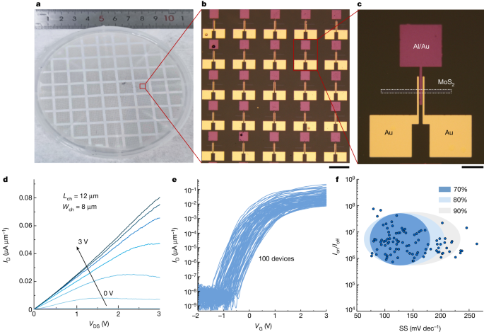
To further demonstrate the scalable fabrication of large-area top-gate FETs, the FET arrays are prepared on a 4-inch chemical vapour deposition(CVD)-MoS2 wafer. The photograph of the 4-inch CVD-MoS2/sapphire wafer with the top-gate FET arrays in Fig. 4a confirms that the complete FET stack is transferred to the MoS2/sapphire substrate. Figure 4b,c does not show any wrinkles or cracks. The typical output curves of these transistors demonstrate excellent electrostatic control of the channel because of the high-quality dielectrics (Fig. 4d). The transfer curves of 100 MoS2 FETs exhibit the typical n-type characteristics with excellent uniformity (Fig. 4e). The statistical distributions of the on/off current ratio (Ion/Ioff) and SS extracted from 100 devices are shown in Fig. 4f and further statistical distributions of the key parameters, including the threshold voltage, off-state current and on-state current are shown in Extended Data Fig. 9. Seventy percent of the devices show SS values in the range of 75â175âmVâdecâ1 and Ion/Ioff higher than 106, which are among the best for CVD-MoS2 FET. The value and distribution of SS for MoS2 transistor array can be markedly improved as wafer-scale single-crystalline MoS2 with excellent quality is available and used in the future. The uniformity and scalability of the c-Al2O3/graphene FETs shown in Extended Data Fig. 10 indicate the ability of the fabricating high-performance radio frequency transistors and other complex circuits with c-Al2O3 technique in the future.
a, Photograph of a 4-inch CVD-MoS2/sapphire wafer with top-gate FET arrays. b, Magnified optical image from the red box in a. c, Magnified optical image from the red box in b. d, The typical output curves of c-Al2O3/MoS2 FETs. e, Transfer curves of 100 MoS2 FETs. f, The statistic distributions of the on/off current ratio and SS from 100 devices. Scale bars, 200âμm (b); 50âμm (c).
In conclusion, we have demonstrated the fabrication of single-crystalline Al2O3 as the high-quality dielectric layer for the top-gate 2D transistors. This breakthrough will serve as the foundation for further advancements in the diversity, scalability and manufacturability of single-crystalline oxides, facilitating the seamless transition of 2D semiconductors from laboratories to industrial environments. The approach for the growth of wafer-scale single-crystalline aluminium and aluminium oxide can be further extended to other metals, and some single-crystalline oxides that were unattainable before can be synthesized for various applications. A notable advancement in this journey is the ability to scale up to the current silicon wafer diameter because the starting germanium for single-crystalline graphene synthesis can be epitaxially grown on silicon directly, which markedly broadens the potential for integration into established silicon-factory manufacturing processes. Meanwhile, the development of an automated debonding-transfer tool dedicated to low-dimensional materials, including single-crystalline dielectric oxide, 2D channel material and ultrathin metal electrode, is crucial to achieve the unique alignments between them for multifunctional 2D devices and is expected to substantially increase throughput, improve reproducibility and enhance the reliability of 2D integrated circuits. By constructing complex 2D integrated circuits, particularly for hetero-integration on mature Si-CMOS platforms, the immense potential of 2D materials can be fully unlocked and can lay the groundwork for the next generation of high-performance electronic devices.


